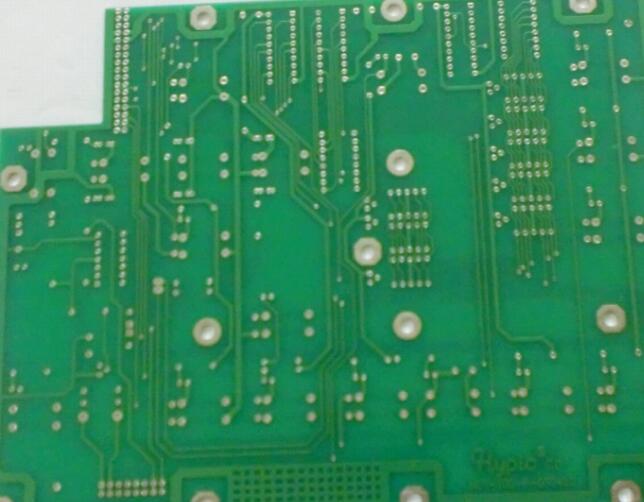
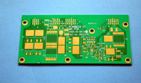
In the production of PCB boards, we often encounter a lot of design reasons that the finished product does not meet the expected design. As a PCB board manufacturer, the film is designed by the customer and printed on the PCB board. If it is a problem with the drawing, the PCB board manufacturer is also powerless. Today, I will give an example of the problems we often encounter in production. How designers should design. Here are some examples. The most likely problems, but there are also some minor problems, but the design does not care so much, which leads to problems. ..
.
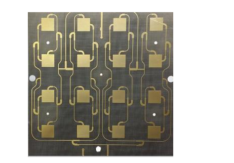
1.The problem of golden hands opening windows: usually our golden fingers are used to open windows. If you want to open the window, you must design the drawing to open the window when designing, not to cover the oil. Because not all engineering personnel will confirm with you when the circuit board manufacturer produces, according to the data production or open the window processing.
.
.
.
2. Via-hole cover oil problem: I often encounter customer complaints. My board needs to be covered with oil. Why is the window open? We checked the design drawings. As a result, the drawings were window-opened. For those that need to cover oil, When designing, it must be designed to be covered with oil, and the window cannot be opened. If you did not notice that you opened the window, the finished product must also be windowed.
For those that must open the window as a test point, please be careful not to cover the oil.
3. Character problems: We often encounter the problem that the characters are too small to be printed. If they are too small, they will be printed as one piece and cannot be seen clearly. The minimum character size required by PCB board manufacturers is 0.8*1.5MM. The minimum size is this size, and it will be unclear if it is smaller than the size. The other is that the characters cannot be placed on the pads, and all the characters on the pads need to be removed.
4. Via-to-line, via-to-hole issues: In the design, at least a 0.2mm spacing between vias and lines must be ensured, and a 0.3mm spacing between holes and holes. In the production process, vias, pads, and lines are all Need compensation. The original drawings need to be spaced to facilitate compensation in the processing of the production drawings. If the production drawings are not compensated, the finished product will be smaller than the design after etching.
5. Distance from hole and line to board edge: It is often encountered that some design holes and lines are next to the contour line. Generally, the distance between the line and the shape should be kept above 0.5mm to ensure that the line has position compensation and the shape will not reach the line when making the shape. The hole to the outer profile line is above 0.5mm, and position compensation is reserved. Less than 0.5MM will cause the edge of the finished product
6.Expose copper: if the edge of the board does not accept exposed copper, it needs to be processed by copper extraction, and the pad will be slightly smaller after copper extraction.
The above are the issues that need to be paid attention to inPCB board design, and I hope to help everyone.