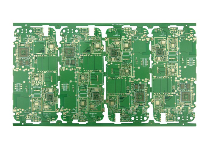
What problems will you encounter when designing PCB samples? The following is a summary of ten problems that are easy to encounter in PCB board proofing design.
Common problems in PCB proofing design

1. Pad overlap
The overlap of the pads means the overlap of the holes. In the drilling process, the holes will be damaged due to multiple drilling in one place, resulting in scrapping.
2. Graphics layer abuse
Specific performance: Some useless connections were made on some graphic layers. The original four-layer board was designed with more than five layers of wiring, which caused misunderstanding; violation of conventional design, such as the component surface design on the Bottom layer and the welding surface design In Top, it causes inconvenience and so on, so the graphic layer is kept intact and clear when designing.
3. Random characters
Specific performance: SMD solder pads for the character cover pads bring inconvenience to the continuity test of the PCB board and the soldering of the components; the character design is too small, causing difficulties in screen printing; too large will make the characters overlap and difficult to distinguish.
4. single-sided pad aperture setting
Single-sided pads are generally not drilled. If the drilled holes need to be marked, the hole diameter should be designed to be zero. If the numerical value is designed, then when the drilling data is generated, the coordinates of the hole appear at this position, and there is a problem.
5. use filler blocks to draw pads
When designing the circuit, it can pass the DRC inspection, but it is not good for processing. When the solder resist is applied, the area of the filler block will be covered by the solder resist, which makes it difficult to solder the device.
6. There are too many filler blocks in the design or the filler blocks are filled with very thin lines
Easily lead to: the phenomenon of light drawing data loss, incomplete light drawing data or considerable amount of light drawing data generated, which increases the difficulty of data processing.
7.the pad design is too short
This is for continuity testing. For surface mount devices that are too dense, the spacing between the two pins is quite small, and the pads are also quite thin. The test pins must be installed in a staggered position up and down (left and right). If the design of the pad is too short, although it will not affect the device installation, it will make the test pins not staggered.
8. Large area grid spacing is too small
The large-area grid spacing is too small (less than 0.3mm), during the PCB board manufacturing process, after the image transfer process, it is easy to produce a lot of broken films attached to the board, causing disconnection.
9. the large area of copper foil is too close to the outer frame
The distance between the large area copper foil and the outer frame should be at least 0.2mm, otherwise it is easy to cause the copper foil to warp and the solder resist falling off caused by it.
10,.the shaped hole is too short
The length/width of the special-shaped hole should be ≥2:1, and the width should be less than 1.0mm; otherwise, the drilling machine will easily break the drill when processing the special-shaped hole, which will cause processing difficulties and increase costs.
The above are ten problems that are easy to encounter when PCB board proofing design. Do you understand all of them? Ipcb also provides PCB manufacturing and printing, PCB board design technology, etc.