How is a high-quality PCB board made?
Today in the era of mobile internet, electronic products such as mobile phones and tablets have become "standard equipment" in people's daily lives. Behind this variety of products, a PCB board that is often overlooked plays a wonderful role-components of various colors are interconnected on the board to build modules and products with different functions, making the electronic world full of infinite possibilities. So, as an engineer, how much do you know about PCB boards? How is the PCB boardmade? Where is the secret of advanced process technology? In view of this, the editor followed in the footsteps of the Blite engineers to visit the Blite factory, and came to the site to find out and understand the secrets behind the PCB board.
Shenzhen Bright Technology Co., Ltd. is mainly positioned in smt patch proofing, PCBA model processing, engineering trial production sample patch, urgent circuit board patch, small and medium batch SMT patch processing and other model welding business. Compared with other factories, Bailit has five major advantages: 1. High-precision configuration, rationalized automatic production line configuration and high-precision equipment configuration are conducive to ensuring the quality of products. ; 2. Rationalization and production line, according to the type of customer's product to select the appropriate production line corresponding to the production, is conducive to reducing production costs. ; 3. High-quality resources, the use of the least personnel and optimized engineering design, can respond to changes in the number of customer orders at any time. 4. Efficient response, with a complete response mechanism and the ability to quickly deal with customer complaints. The Bright factory in Shiyan is clean and open, with excellent lighting effects.
When I came to Bright’s door, the first thing I saw was the tall front desk.
front desk

Entering from the front desk is a spacious office.
Just as the editor asked about the related questions about the circuit board, the engineer of Blite explained the relevant knowledge to the editor.
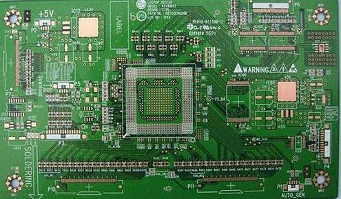
Cutting is the first step in the production of PCB boards. According to the requirements of the pre-production design and planning, the substrate is cut to the required size to avoid the edge burrs from affecting the quality. After cutting, edge grinding and rounding are required. After cutting the material, use a drilling machine to drill through holes that connect the lines between the layers. After drilling, the PCB is chemically deposited on the surface with a thickness of 20-40 microinches of chemical copper. After copper sinking, the PCB board needs to be plated with 200-500 micro-inch thick copper to protect the 20-40 micro-inch thick chemical copper from being damaged by the subsequent process and causing hole breakage.
Machine at work
How is the circuit covered on the copper plate? In the darkroom, the staff prints the PCB circuit diagram on the film, and transfers the image to the photosensitive base plate through light irradiation. The light-transmitting part undergoes photopolymerization, the opaque part does not react, and the reacted part cannot be dissolved during development. And keep it on the board. During development, the dry film that has not undergone polymerization reaction is washed away with an alkaline solution, and the dry film that has undergone polymerization reaction remains on the surface of the board as a protective layer during etching.
The engineer showed the product in processing to the editor.
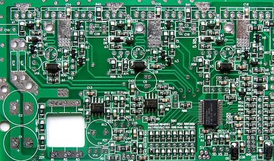
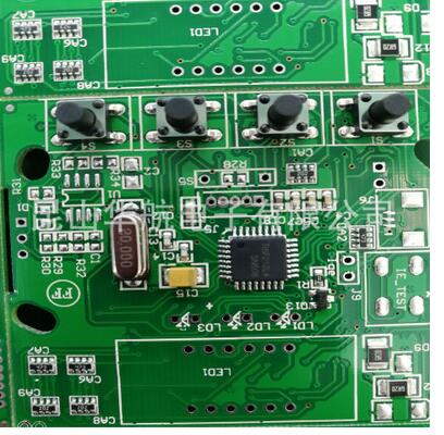
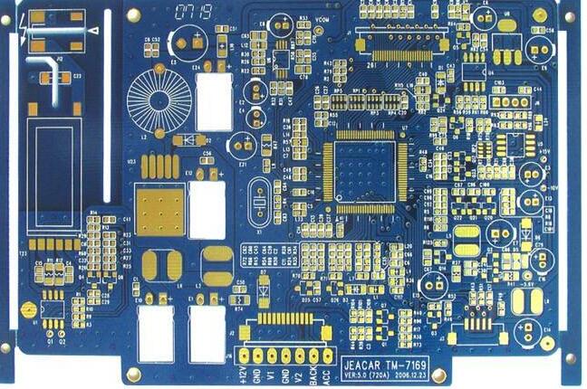
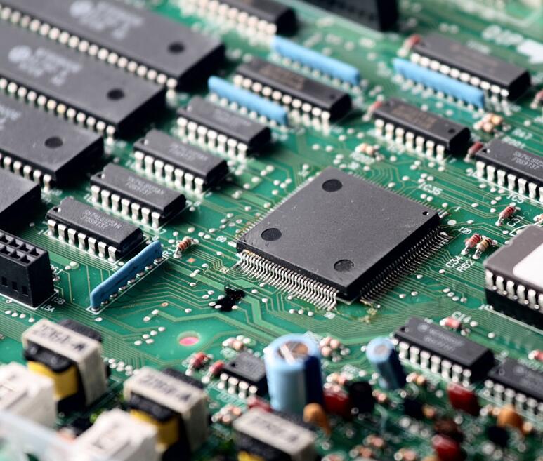
PCB boards are neatly stacked together
The exposed copper surface after development needs to be copper-plated twice to achieve the copper thickness required by the customer. A layer of tin protection is plated on the surface of the secondary copper plating as a protective agent during etching.
During etching, the PCB board is sprayed with a certain pressure of etching solution through the etching machine, and the exposed copper is corroded by the solution to form a circuit pattern, and then the protective tin layer is removed by the tin stripping machine to expose the circuit pattern.
The etched PCB board needs to undergo AOI (Automatic Optical Inspection). The image is fed back to the equipment for processing through the principle of optical reflection, and the defect is found and repaired by comparing it with the data pattern. After AOI scanning and repairing, the PCB pass-through rate Will reach more than 99.9%.
After the AOI process, the PCB board will be returned to the clean room as a solder mask layer, commonly known as "green oil". This layer of ink covers the unexpected lines except for the pads, which can avoid soldering open circuit during the use of the PCB board and prolong the service life of the PCB. . In order to facilitate visual inspection, more green pigments are added to the main paint that are helpful to the eyes. In addition to green, there are yellow, blue, red, white, black and other colors.
After the surface treatment of the PCB, the large board will be assembled and the small board will be divided by a high-speed gong machine
PCB board flying probe test, check whether there is a short circuit or open circuit on the board
The flying probe test does not need to make expensive jigs. Use two probes to move the x, y, and z axes to test the two ends of each circuit one by one. Its advantages include: rapid test development, low cost, flexible conversion, and rapid feedback for designers in the prototype stage. Through the previous double check of AOI and flying probe test, it can guarantee 100% pass rate of PCB board.
Afterwards, the engineer gave some thoughts to the editor. He said that the company will continue to increase investment, introduce advanced equipment and advanced technology, and introduce high-end talents to continuously improve the factory's technological capabilities and service level, while also integrating resources and enhancing effectiveness. Bright will make unremitting efforts to shorten the product development cycle and reduce the cost of research and development for Chinese electronics companies, and contribute its own strength to the innovation of China's electronics industry.
According to reports, PCB is one of the 15 key development areas of my country's electronic information industry in the next 5 to 15 years. In recent years, the electronic information industry has developed rapidly, but the PCB industry lags behind the growth rate of the electronic information industry. The output is far behind the market and needs to rely heavily on imports. Therefore, the PCB industry has a lot of room for growth in the future. Bright adapts to the development trend of today's era, builds a brand-new PCB industry with Internet thinking, eliminates cumbersome processes through management systems, process tracking, etc., and improves customer experience. The editor also discovered during the visit that the Bailit factory has strict management and demanding details. Those who enter the factory are required to wear shoe covers to prevent external dust from polluting the PCB board. Through accurate positioning planning and advanced management mode, every customer will be satisfied.