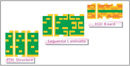
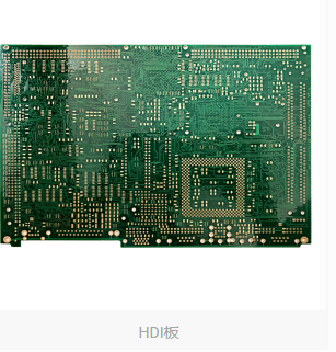
What is the first-order and second-order HDI-PCB board?
1. With one-time support, with one-time support for copper foil
2. Drill the hole into the hole. When crushing, press the copper foil. You have to see how many lasers you have, and how many orders is this
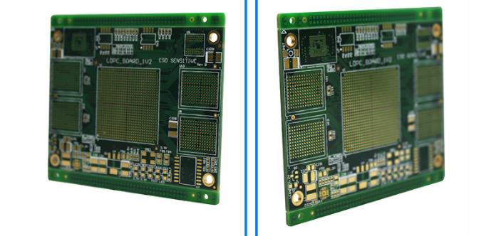
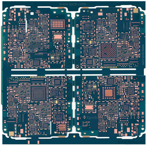
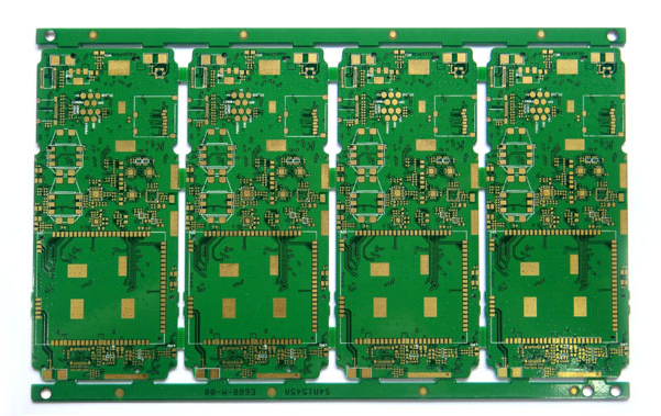
3. Basic knowledge and production process With the rapid changes in the electronics industry, electronic products have made progress in brilliance, lightness, miniaturization and miniaturization. Corresponding printed circuit boards must also face the challenges of high-precision circuit boards, fine linearization and high density.
The trend of printed circuits in the global market is to introduce climax and burial in high-density interconnect products, thereby gaining positions more effectively and reducing the width and spacing of lines.
4. Definition of Human Development Report
HDI: Abbreviation: high-density, high-density interconnection, non-mechanical drilling, climax microporous ring less than 6 meters, wiring spacing between inner and outer layers less than 4 meters, and its diameter does not exceed 0.35 mm, called HDI board.
Brincon: Through the Braille abbreviation linked to the inner and outer layers.
The way to achieve connection and conduction between the inner layer and the inner layer The large holes are mainly small holes with a diameter of 0.05 mm to 0.15 mm. The circular hole is formed by laser, plasma etching and induction inductance.
Laser holes are usually formed by lasers.

Laser holes are divided into CO2 and ultraviolet lasers (UV).
Plank
1. HDI A RCC, LDPE, FR4
(1) RCC: Copper coated with resin, copper foil made of resin. CDC is composed of copper foil and resins that are cured, heat-resistant and oxidation-resistant. Its structure is shown in the figure below: (in thickness> 4 meters)
2. The RCC resin layer has the same technical characteristics as FR-4 (PPRPREG).
In addition, it also meets the performance requirements of stacked multi-layer cards, such as:
(1) High insulation reliability and micropore reliability;
(2) High glass transition temperature (Tg);
(3) Low dielectric constant and low absorption; it has high strength and resistance to copper foil.
(5) Uniform filling of the insulating layer after curing. At the same time, RCC is a new product without glass fiber, which is conducive to laser engraving, plasma, thin plates and thin plates. In addition, the resin-coated copper foil has a sheet of 12H, 18H, a thin copper foil that is easy to handle.
3. LDPE:
(3) FR4 (FR4): thickness <= 4 meters. Generally use PP 1080, try not to use 2116 pp
2. Copper foil specifications: when customers do not need it, the copper foil on the substrate is more suitable for 1 ounce than the traditional printed circuit board, HDI and traditional internal and external electrolytic copper foil in 1/3 OZ.
Laser holding: CO2 and laser YAV Laser hole formation principle: The laser beam is a laser beam, which is stimulated by external stimulation. When the "radius" is stimulated by higher and higher energy, infrared or visible light has heat energy. The ultraviolet light has a characteristic.
Chemical. Reflection, absorption, and transmission are three phenomena that occur when shooting on the surface of the work object, of which only the absorbent can play a role.
The effect of photothermal ablation can be divided into two different reactions: photothermalization and photochemical cracking.
1. Hole forming of ultraviolet laser: it can collect small beams, and the absorption rate of copper foil is relatively high. It can take off the copper foil and burn the micro-holes below 4 meters.
Compared with the formation of a carbon dioxide laser, there is no resin at the bottom of the hole, but the copper foil is easily damaged at the bottom of the hole. The energy of a single pulse is very low and the treatment efficiency is low.
(YAG, UV: Wavelength: 355, the wavelength is very short, it can handle very small holes, and can be absorbed by resin and copper at the same time), no special process of opening the window is required.
2. Laser 2. CO2 waveband formation: using CO2 infrared laser, CO2 can not be absorbed by copper, but can absorb resin and glass fibers, usually 4 to 6 meters of micropores.
This is an important question.
A. Standard-compliant mask with bronze window opening method First, we must use the internal control card on the RCC map, then open the window, and then use laser light to burn the substrate in the window to supplement the orgasm micro-holes.
The details are as follows: First, the FR-4 core card is to have narrow lines and targets (target bags) on both sides, and then squeeze them together.
Then, according to the position of the climax hole, the corresponding copper skin is withdrawn according to the confirmed copper window film, and then the window resin is burned with a CO2 laser, so that the bottom of the bottom can be melted to form a micro-hole.
This law was originally issued by Hitachi Manufacturing Institute. In general, if a manufacturer wants to ship its products to the Japanese market, then it may need to pay attention to legal issues.
B. Large mask and large bronze window The "open window method" involves comparing a copper window of about 1,000 inches with the side of the Bolman hole. Generally speaking, if the bid opening is 6 meters, the large window can be opened within 8 minutes.
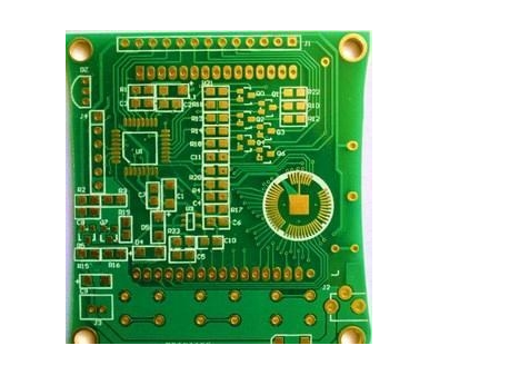
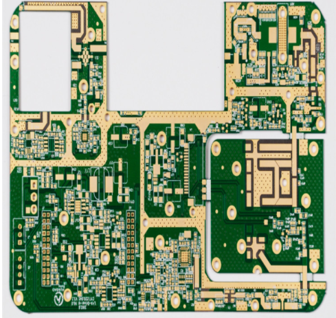
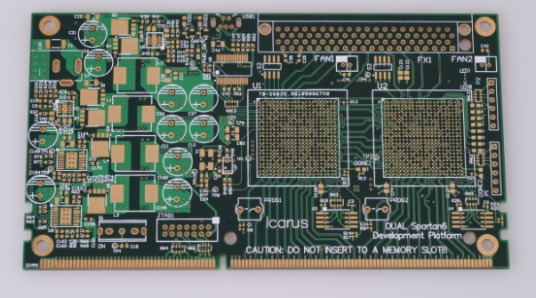
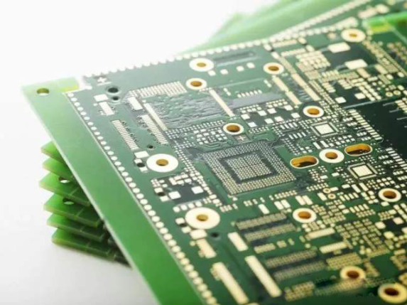
ipcb is a high-precision, high-quality PCB manufacturer, such as: isola 370hr PCB, high-frequency PCB, high-speed PCB, ic substrate, ic test board, impedance PCB, HDI PCB, Rigid-Flex PCB, buried blind PCB, advanced PCB, microwave PCB, telfon PCB and other ipcb are good at PCB manufacturing.