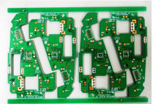
PCB copper treatment experience
PCB manufacturer: Copper cladding refers to using the free space on the PCB as a reference level, and then filling it with solid copper, also known as copper filling.
The significance of copper plating is to reduce the ground impedance, improve the anti-interference ability, reduce the voltage drop, improve the power efficiency, and connect to the ground wire to reduce the loop area.
If PCBs such as SGND, AGND, GND, etc., how to coat copper?
My method is to use the most important "ground" as the reference for the copper plating layer according to the different positions of the PCB board, and perform digital and analog copper plating.
Separate.
At the same time, before copper plating, the corresponding power supply wiring should be coarsened: V5.0V, V3.6V, V3.3V (SD card power supply). This forms many polymorphic structures with different shapes.
The copper cladding needs to solve several problems: one is the single-point connection in different places, and the other is the copper cladding near the crystal oscillator.

The crystal oscillator in the circuit is a high-frequency transmitter. The method is to deposit copper around the crystal oscillator, and then grind the crystal oscillator housing separately.
Thirdly, the issue of islands (dead zones), if it feels great, you don't need to define many places to increase passage holes. In addition, large-area copper plating or grid copper plating has a better effect and is not suitable for promotion.
Why? Large area copper plating, if wave soldering, the board may warp or even blisters.
From this point of view, the grid has better heat dissipation performance. Generally speaking, high-frequency circuits have high requirements on the anti-interference of multi-purpose power grids, while low-frequency circuits have ordinary copper roads, such as high-current circuits.
Add to: In digital circuits, especially in microcontroller circuits, the role of copper plating is to reduce the impedance of the entire ground.
Specifically, I usually do this: each core module (including digital circuits), if possible, is divided by copper, and then each copper coating is connected by wires.
The purpose of doing so is also to reduce the impact between various levels of circuits.
For hybrid circuits of digital and analog circuits, the final sum of filter capacitors for independent wiring of the ground wire is well known.
However, there is one thing: the ground wire distribution of an analog circuit cannot simply be covered with a piece of copper. Since the analog circuit pays more attention to the interaction between the front and the back, and the analog grounding also needs a single-point grounding, whether the analog copper plating can be applied must be dealt with according to the actual situation. (This requires some special characteristics of the analog integrated circuit used)
iPCB is a high-tech manufacturing enterprise focusing on the development and production of high-precision PCBs. iPCB is happy to be your business partner. Our business goal is to become the most professional prototyping PCB manufacturer in the world. Mainly focus on microwave high frequency PCB, high frequency mixed pressure, ultra-high multi-layer IC testing, from 1+ to 6+ HDI, Anylayer HDI, IC Substrate, IC test board, rigid flexible PCB, ordinary multi-layer FR4 PCB, etc. Products are widely used in industry 4.0, communications, industrial control, digital, power, computers, automobiles, medical, aerospace, instrumentation, Internet of Things and other fields.