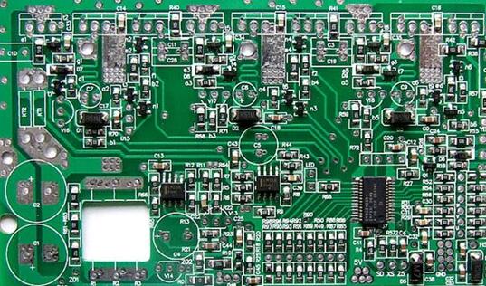
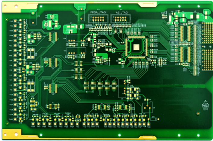
What rules should be followed in the layout of PCB components?
In PCB proofing design, component layout is an important part.
PCB engineers have their own set of standards on how to lay out components correctly and effectively. For most component layouts, the following 10 rules need to be followed.
1. According to the layout principle of "big first, small first, easy first", that is, priority is given to the layout of important unit circuits and core components.
2. The layout should refer to the principle block diagram, and the main components should be arranged according to the flow pattern of the main signal of the plywood.
3. The layout of the components should be easy to debug and maintain. In other words, there should be enough space around small components, and there should not be enough space around large components that need to be debugged.
4. For the same circuit structure, a symmetrical standard layout should be adopted as much as possible.
5. Optimize the layout according to the evenly distributed standard, balance the center of gravity and beautiful layout.
6. Filter elements of the same type should be placed in one direction along the X or Y direction. In order to facilitate production and testing, the same type of polar discrete components should also strive to maintain consistency in the X or Y direction.

7. Heating elements should generally be evenly distributed to facilitate heat dissipation of the single board and the whole machine. In addition to temperature detection components, temperature-sensitive devices should be kept away from high-calorific components.
8. The layout should meet the following requirements as much as possible: the total connection should be as short as possible, and the key signal line should be the shortest; the weak signals of high voltage, large current, and small current are completely separated; the analog signal is separated from the digital signal; the high frequency signal and the low frequency signal are separated Frequency signal; and high frequency components are completely separated.
9. The decoupling capacitor should be as close as possible to the IC power supply pin, and the circuit formed between the power supply and the ground should be as short as possible.
10. When placing components appropriately, consider combining them as much as possible for future power separation.
iPCB is a high-tech manufacturing enterprise focusing on the development and production of high-precision PCBs. iPCB is happy to be your business partner. Our business goal is to become the most professional prototyping PCB manufacturer in the world. Mainly focus on microwave high frequency PCB, high frequency mixed pressure, ultra-high multi-layer IC testing, from 1+ to 6+ HDI, Anylayer HDI, IC Substrate, IC test board, rigid flexible PCB, ordinary multi-layer FR4 PCB, etc. Products are widely used in industry 4.0, communications, industrial control, digital, power, computers, automobiles, medical, aerospace, instrumentation, Internet of Things and other fields.