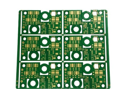
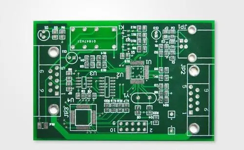
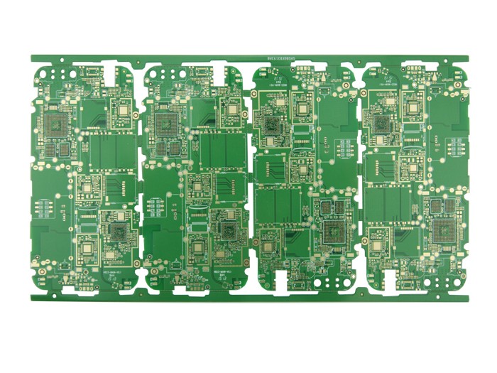
Although printed circuit board(PCB) wiring plays a key role in high-speed circuits, it is often one of the last few steps in the circuit design process. There are many problems with high-speed PCB wiring, and a lot of literature has been written on this topic. This article mainly discusses the wiring of high-speed circuits from a practical perspective. The main purpose is to help new users draw attention to many different issues that need to be considered when designing high-speed circuit PCB wiring. Another purpose is to provide a review material for customers who have not touched PCB wiring for a while. Due to the limited layout, this article cannot discuss all the issues in detail, but we will discuss the key parts that have great results in improving circuit performance, shortening design time, and saving modification time.

Although this is mainly for circuits related to high-speed operational amplifiers, the problems and methods discussed here are generally applicable to wiring used in most other high-speed analog circuits. When the operational amplifier works in a very high radio frequency (RF) frequency band, the performance of the circuit largely depends on the PCB layout. The high-performance circuit design that looks good on the "drawing" can only get normal performance if it is affected by carelessness and carelessness in wiring. Pre-consideration and attention to important details during the entire wiring process will help ensure the expected circuit performance.
Schematic diagram
Although a good schematic diagram cannot guarantee a good wiring, a good wiring starts with a good schematic. Think carefully when drawing the schematic, and you must consider the signal flow of the entire circuit. If there is a normal and stable signal flow from left to right in the schematic, then there should be an equally good signal flow on the PCB. Give as much useful information as possible on the schematic. Because sometimes the circuit design engineer is not there, customers will ask us to help solve the circuit problem, the designers, technicians and engineers engaged in this work will be very grateful, including us.
In addition to the common reference identifier, power consumption and error tolerance, what other information should be given in the schematic? Here are some suggestions for turning ordinary schematics into first-class schematics. Add waveforms, mechanical information about the casing, length of printed lines, blank areas; indicate which components need to be placed on the PCB; give adjustment information, component value ranges, heat dissipation information, control impedance printed lines, comments, and brief circuits Action description...and others.