In the process of transferring the inner layer circuit pattern from the base material to several times of pressing to the outer layer circuit pattern transfer, the warp and weft direction of the jigsaw will be different.
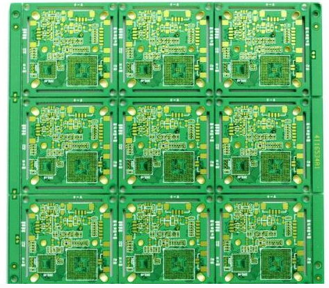
From the entire PCB production FLOW-CHART, we can find out the reasons and procedures that may cause abnormal expansion and shrinkage of the board and poor dimensional consistency:
1. The dimensional stability of the incoming material of the substrate, especially the dimensional consistency between each laminated CYCLE of the supplier; even if the dimensional stability of the same specifications of the substrates of different CYCLEs is within the specifications, but because of the consistency between them Poor performance, which can cause the first board trial production of the board to determine a reasonable inner layer compensation. The difference between different batches of boards causes the graphic size of the subsequent mass production boards to be out of tolerance; at the same time, there is another material abnormality. After the transfer of the outer layer graphics to the shape process, the board was found to shrink; during the production process, there were individual batches of boards. During the data measurement process before the shape processing, it was found that the width of the panel was relative to the length of the shipping unit. The transfer magnification showed serious shrinkage, and the ratio reached 3.6mil/10inch. The specific data is shown in the following table; after tracing, the X-RAY measurement of the abnormal batch of panels after the outer layer lamination and the outer pattern transfer magnification are both within the control range. Yes, there is still no better method for monitoring in process monitoring;
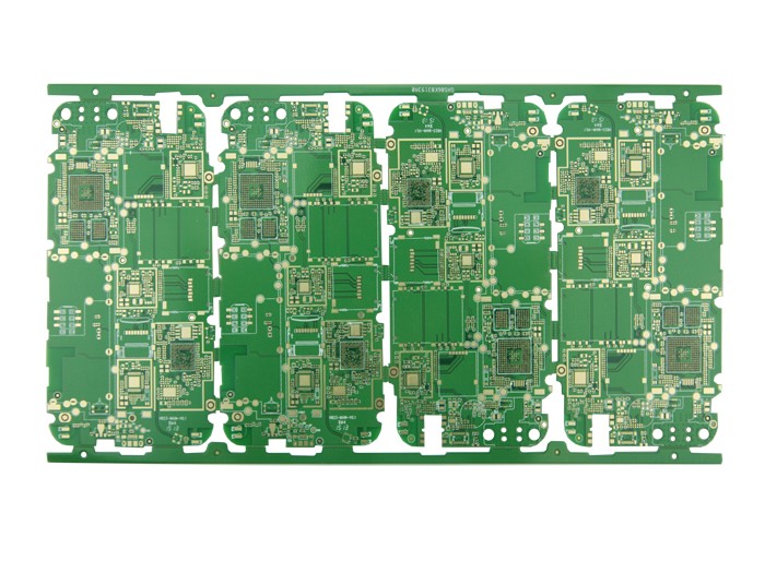
2. Panel design: The panel design of conventional panels is symmetrical, and there is no obvious impact on the graphic size of the finished PCB when the graphics transfer rate is normal; In the process of cost, the design of asymmetric structure is used, which will have a very obvious impact on the consistency of the figure size of the finished PCB in different distribution areas. We can even drill blind holes in the laser during the PCB processing. In the process of hole and outer pattern transfer exposure/solder resist exposure/character printing, it is found that the alignment of such asymmetrically designed plates in each link is more difficult to control and improve than conventional plates.

3. An inner layer graphics transfer process: This is a very critical role in whether the size of the finished PCB board meets customer requirements; for example, there is a large deviation in the film magnification compensation provided for an inner layer graphics transfer, which can not only directly lead to the finished PCB In addition to the pattern size that cannot meet customer requirements, it can also cause the subsequent alignment of the laser blind hole and its bottom connecting plate to cause a decrease in the insulation performance between the LAYER TO LAYER and even a short circuit, as well as the through/blind hole alignment during the transfer of the outer layer pattern. problem;
Based on the above analysis, we can take appropriate measures to monitor and improve abnormalities;
1. Monitoring the dimensional stability of incoming substrates and the consistency of sizes between batches: Regularly conduct dimensional stability tests on substrates provided by different suppliers to track the difference in latitude and longitude data between different batches of the same specifications, And can use statistical techniques to analyze the test data of the substrate; thus, it can also find suppliers with relatively stable quality, and provide more detailed supplier selection data for SQE and purchasing departments; for the basis of individual batches The poor dimensional stability of the material causes serious expansion and contraction of the board after the transfer of the outer layer graphics. At present, it can only be found by the measurement of the first board of the shape production or the measurement during the shipment review; but the latter has higher requirements for batch management. Mixed boards are prone to occur during mass production of a certain number;
2. In terms of panel design, a symmetrical structure should be adopted to ensure that the expansion and contraction of each shipping unit in the panel is relatively consistent; if possible, communicate with the customer to suggest that it allows etching/ Characters and other identification methods specifically identify the location of each shipping unit in the puzzle; this method will have a more obvious effect in the asymmetrical design of the board, even if the size of each unit is oversized due to the asymmetry of the graphics in each puzzle. Even the abnormal connection at the bottom of the partial blind hole caused by this can be very convenient to determine the abnormal unit and pick it out before shipment, so that it will not flow out and cause the customer to package abnormally and cause complaints;
3. Make the first board of magnification, and use the first board to scientifically determine the one-time inner layer graphics transfer magnification of the production board; this is particularly important when changing the substrate or P-film of other suppliers to reduce production costs; When the board is out of the control range, it should be processed according to whether the unit pipe position hole is secondary drilling; if it is a conventional processing flow, the board can be released to the outer layer according to the actual situation and transferred to the film magnification for appropriate adjustment; if it is a secondary drilling For orifice parts, special care must be taken in the treatment of abnormal panels to ensure that the graphic size of the finished panel and the distance from the target to the pipe position hole (secondary drilling); a collection list of the first board magnification of the secondary laminated panel is attached;
4. Process monitoring: Use the target data of the inner layer of the plate measured when the X-RAY of the outer layer or sub-outer layer is laminated to produce the drilling pipe position hole, and analyze whether it is within the control range and is consistent with The corresponding data collected by the qualified first board is compared to determine whether the board size has abnormal expansion and contraction. The following table is available for reference; after theoretical calculation, usually the magnification here should be controlled within +/-0.025% to meet the conventional board The size requirements of the pieces;
Through analyzing the reasons of PCB size expansion and shrinking, find out the available monitoring and improvement methods, hoping that the majority of PCBpractitioners can get enlightenment from it and find the improvement plan that suits their company based on their actual situation.