Introduction: I believe everyone is familiar with the PCB board, but do you know the PCB board design process?

1. Introduction to the circuit board
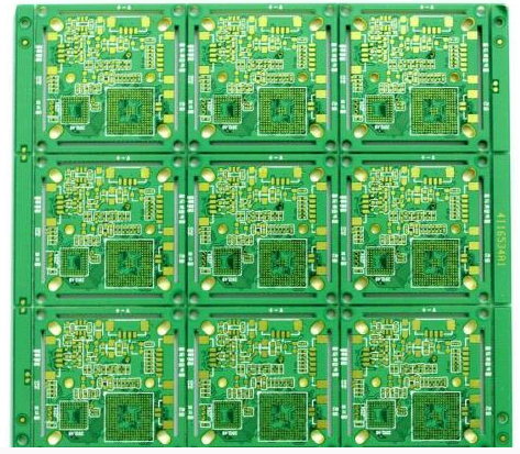
Printed Circuit Board (PCB), also known as circuit board, PCB board, aluminum substrate, high-frequency PCB, ultra-thin circuit board, ultra-thin circuit board, printed (copper etching technology) circuit board, etc., is important Electronic components are the support of electronic components and the provider of the circuit connection of electronic components. The traditional circuit board uses the method of printing etching resist to make the circuit lines and drawings, so it is called a printed circuit board or a printed circuit board. Due to the continuous miniaturization and refinement of electronic products, most of the current circuit boards are attached with etching resists (laminated or coated), and after exposure and development, the circuit boards are made by etching.
2. The components of the circuit board
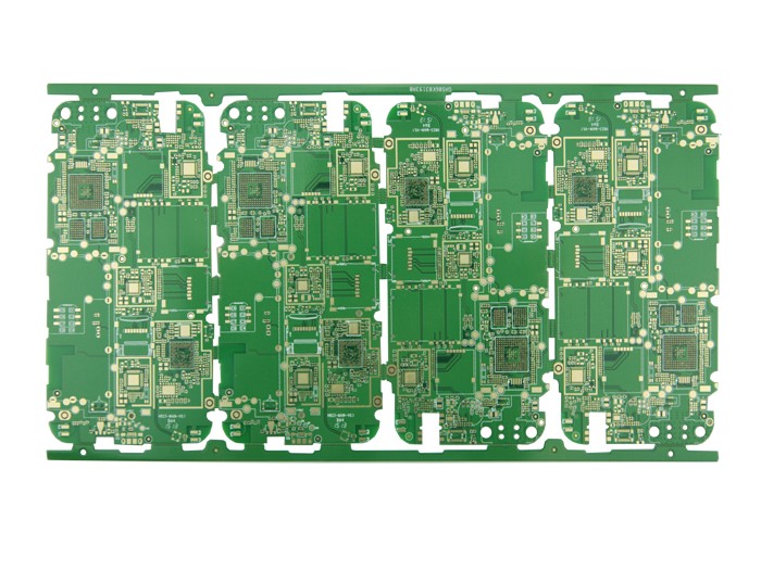
The circuit board is mainly composed of pads, vias, mounting holes, wires, components, connectors, filling, electrical boundaries, etc. Common layer structures include single layer PCB (Single Layer PCB), double layer PCB (Double Layer PCB) and multi-layer PCB (Multi Layer PCB). The main functions of each component are as follows:
Pad: A metal hole used for soldering component pins.
Vias: There are metal vias and non-metal vias. Metal vias are used to connect component pins between layers.
Mounting hole: used to fix the circuit board.
Wire: The copper film of the electrical network used to connect the pins of the components.
Connectors: components used to connect between circuit boards.
Filling: Copper coating for ground wire network, which can effectively reduce impedance.
Electrical boundary: used to determine the size of the circuit board, all components on the circuit board cannot exceed the boundary.
3. Introduction to the circuit board design process
The working principle of the circuit board: is to isolate the conductive layer of copper foil on the surface by using the board-based insulating material, so that the current flows in various components along the pre-designed route to complete tasks such as work, amplification, attenuation, modulation, demodulation, and encoding. And other functions.
On the most basic PCB, the parts are concentrated on one side, and the wires are concentrated on the other side. Because the wires only appear on one side, this kind of PCB is called a single panel. For multi-layer boards, multiple layers have wires, and there must be a proper circuit connection between the two layers. This kind of bridge between circuits is called a via. The basic design process of the circuit board can be divided into the following four steps:
(1) The design of the circuit schematic diagram-The design of the circuit schematic diagram mainly uses the schematic diagram editor to draw the schematic diagram, such as Orcad.
(2) Generate a network report --- The network report is a report that shows the link relationship between the circuit principle and the various components in it. It is the bridge and tie connecting the circuit schematic design and the circuit board design. Through the network report of the circuit schematic, You can quickly find the connection between the components, so as to provide convenience for the subsequent PCB design.
(3) The design of the printed circuit board---the design of the printed circuit board is what we usually call the PCB design. It is the final form of the circuit schematic. The related design of this part is larger than the circuit schematic design. We can use the powerful design functions of Allegro, Pads and other software to complete this part of the design.
(4) Generate printed circuit board reports---After the printed circuit board design is completed, various reports need to be generated, such as generating pin reports, circuit board information reports, network status reports, etc., and finally print out the printed circuit diagram.