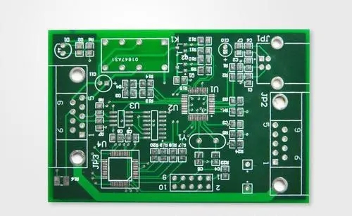
To make a design, the first thing a designer needs to do is to have a rough overall layout so that a specific design plan can be made. The same is true for PCB design. To make the PCB board look like you want, the overall layout and the placement of components are the first considerations. They play a key role in the design of the PCB board, and they directly affect the entire printed circuit. PCB board installation, reliability, ventilation and heat dissipation, and the straight-through rate of wiring.

a. Outer layer size. When the size is too large, the printed lines will be long, the impedance will increase, the anti-noise ability will decrease, and the cost will increase; if the size is too small, the heat dissipation will not be good, and adjacent lines will be easily disturbed. Therefore, we must first make a reasonable positioning for the size and shape of the PCB.
b. The location of special components and unit circuits, etc. The whole circuit should be divided into several unit circuits or modules according to the circuit process, and the core components of each unit circuit should be the center, and the other components should be arranged evenly, neatly and compactly on the PCB board in a certain order. Can't get too close
c. Large components, especially relatively large and tall components, must have a certain distance, which is helpful for soldering and rework.
d. For integrated circuits with higher power, consider color heat sinks, leave enough space, and place them in a well-ventilated and heat-dissipated location. At the same time, don't be too concentrated, have a certain distance, and keep them in the direction of 45 angles.
e. Some smaller integrated circuits should be arranged in the axial direction, and the resistance-capacitance components should be arranged in the vertical axial direction. All these directions are relative to the transfer direction of the PCB production process. The regular arrangement of components will reduce defects in welding.
f. Light-emitting diodes for display, etc., are used for observation during the application process and can be placed on the edge of the printed board.
g. Switches, fine-tuning components, etc. should be placed in an easy-to-operate place.
h. In the same frequency circuit, the distribution parameters between the components should be considered. Generally, the distribution parameters between the components should be considered in the high-frequency circuit. Generally, the components should be arranged in parallel as much as possible in the circuit, which is not only beautiful, but also easy to install and solder., And easy batch production at the same time. The i. components located on the edge of the PCB board must be 3-5 cm away from the edge.
j. At the same time, comprehensive consideration should be given to the thermal expansion coefficient, thermal conductivity, heat resistance and bending strength of the PCB board to avoid adverse effects on the components or PCB during production.
After the above considerations are completed, you can proceed to the next step. This step cannot be underestimated. This is the beginning of a PCB board, which determines what kind of board it will be and what functions it has. One step, so it is necessary to do this step well.