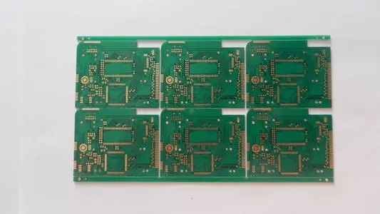
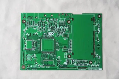
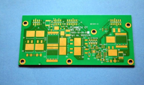
The thing about PCBA processing technology
How much do you know about PCBA processing technology? Jinerte is a professional PCBA processing factory. He is particularly good at PCBA processing technology. He also gave us a comprehensive description of several PCBA process issues:
First: The upper tin position cannot have a silk screen image.
First: The minimum distance between the copper foil and the board edge is 0.5mm, and the minimum distance between the component and the board edge is 5.0mm. The minimum distance between the pad and the board edge is 4.0mm.
Third: The minimum gap of copper foil: 0.3mm for single panel and 0.2mm for double panel.
13. When designing a double panel, pay attention to the components of the metal shell. When the shell is in contact with the printed board when plug-in, the top pad cannot be opened, and it must be covered with solder mask or silk screen oil.

Fourth: Do not place jumpers under the IC or under the components of motors, potentiometers and other large-volume metal casings.
Fifth: The electrolytic capacitor should not touch heating components. Such as high-power resistors, thermistors, transformers, radiators. The minimum distance between the electrolytic capacitor and the radiator is 10mm. The distance between other components and the radiator is 2.0mm.
Sixth: Large-scale components (such as transformers, electrolytic capacitors with a diameter of 15mm or more, high-current sockets.) should increase the pad.
Seventh: The minimum line width of copper foil: 0.3mm for single-sided boards, and the minimum copper foil on the side of 0.2mm for double-sided boards is 1.0mm.
Eighth: There should be no copper foil (except for grounding) and components (or according to the requirements of the structure drawing) within the radius of 5mm of the screw hole.
Ninth: The pad size (diameter) of the general through-hole mounting component is twice the aperture. The minimum double-sided board is 1.5mm, and the minimum single-sided board is 2.0mm. If you cannot use a round land, you can use a waist round land.
Tenth: If the distance between the center of the pad is less than 2.5mm, the adjacent pads must be wrapped with silkscreen oil, and the width of the silkscreen oil is 0.2mm.
Eleventh: Components that need to be soldered after soldering through a tin furnace. The solder pads should be driven away from the tin position. The direction is opposite to the soldering direction. It is 0.5mm to 1.0mm. This is mainly used for single-sided mid-post soldered soldering pads, so as to avoid Blocked when passing the furnace.
Twelfth: In the large-area PCB design(about more than 500cm), in order to prevent the PCB board from bending when going through the tin furnace, a gap of 5mm to 10mm should be left in the middle of the PCB board without components (wires can be routed). Add a bead to prevent bending when passing through the tin furnace.
Thirteenth: In order to reduce the short circuit of the solder joints, all double-sided boards and vias do not open solder mask windows. The Internet era has broken the traditional marketing model, and a large number of resources have been gathered together to the greatest extent through the Internet, which has also accelerated the development speed of FPC flexible circuit boards, and then as the development speed accelerates, environmental problems will continue to appear in PCB factories. In front of him. However, with the development of the Internet, environmental protection and environmental informatization have also been developed by leaps and bounds. Environmental information data centers and green electronic procurement are gradually being applied to the actual production and operation fields.