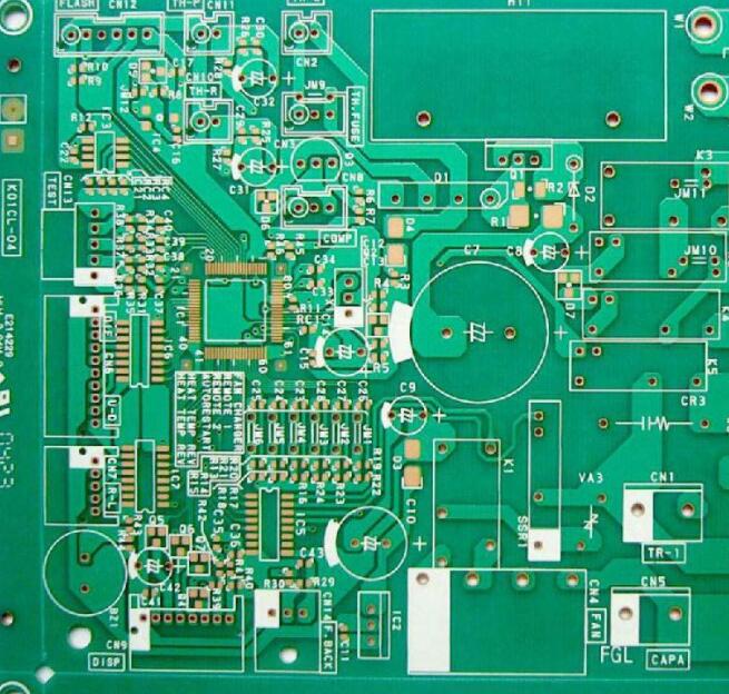
Shenzhen PCBA processing PCB board processing | PCB boarding time
Paying attention to the trend of environmental informationization and the development of various environmental protection technologies, PCB factories can start with big data to monitor corporate pollution and governance results, and find and solve environmental pollution problems in a timely manner. Keep up with the production concept of the new era, continuously improve resource utilization, and realize green production. Efforts to enable the PCB factory industry to achieve an efficient, economical and environmentally friendly production model, and actively respond to the country's environmental protection policy.
Since 2003, the world's electronic circuit industry technology has developed rapidly, concentrated in passive (ie embedded or embedded) component PCB, inkjet PCB technology, optical technology PCB, and the application of nanomaterials on PCB boards.
The development of PCB from mounting substrate to package carrier, as well as the chipization and integration of components, the increasing popularity of BGA (ball grid array), CSP (chip scale packaging) and MCM (multi-chip module) require the PCB package terminal to be fine High integration of packaging and packaging also requires substrates to undertake new functions, and printed boards with embedded components appear to meet the requirements of high-density assembly. Shenzhen PCBA processing

With the development of optical interface technology, in the future, we will establish a modular technology that realizes optical wiring technology, optical printed circuit board technology, optical surface mounting technology, and photoelectric integration on electrical PCBs. With the increasing speed of the system, PCB impedance matching has become an important issue. Depending on the signal speed and wiring length, the distortion is required to be reduced to 10% or 5% or less, or even 3% or less.
In order to meet the development needs of chip scale packaging (CSP) and flip chip packaging (FC), high-density PCBs with internal vias (IVH) structures are required, but its high price limits its use, so it is necessary to reduce costs. At present, the multi-layer process of the build-up method has been adopted to realize the PCB of the IVH structure, and the process of the build-up method is continuously optimized to realize the low-cost mass production of the PCB of the IVH structure.
In order to meet the needs of the development of CSP and FC packaging with fine terminal pitch, the future goal of the conductor pattern miniaturization technology is determined as: the minimum line width/spacing is 25μm/25μm, the wiring center distance is 50μm, and the conductor thickness is less than 5μm. The laser via hole process is the mainstream of the multi-layer board via hole processing methods. CO2 laser and UV laser processing machines have become the mainstream for the development of practical processes. The minimum via hole diameter will be reduced from the current 50 μm to 80 μm. To 30μm, the accuracy of the hole diameter and the position of the via hole are increased to ±15μm. New technologies will likely bring huge changes to the PCB industry.
PCB boards with embedded thin passive components have been used in GSM mobile phones. It is expected that PCB boards with internal IC components and thin-film components embedded in flexible circuit boards will appear in the past two years. A new generation of PCB s made of nano-materials for wiring has appeared for the first time in the world. In the future, it will reduce the dielectric constant of PCBs, improve the heat resistance of products, and have a significant impact on the application of environmental protection in the PCB industry. Shenzhen PCBA processing