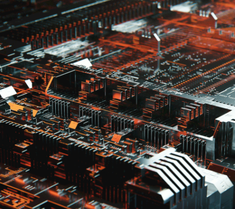
What is the meaning of BGA in PCBA processing
iPCB is happy to be your business partner. Our business goal is to become the most professional prototyping PCB manufacturer in the world. With more than ten years of experience in this field, we are committed to meeting the needs of customers from different industries in terms of quality, delivery, cost-effectiveness and any other demanding requirements. As one of the most experienced PCB manufacturers and SMT assemblers in China, we are proud to be your best business partner and good friend in all aspects of your PCB needs. We strive to make your research and development work easy and worry-free.
quality assurance
iPCB has passed ISO9001:2008, ISO14001, UL, CQC and other quality management system certifications, produces standardized and qualified PCB products, masters complex process technology, and uses professional equipment such as AOI and Flying Probe to control production and X-ray inspection machines. Finally, we will use double FQC inspection of appearance to ensure shipment under IPC II standard or IPC III standard.

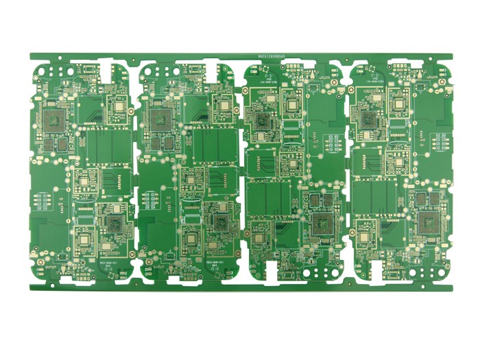
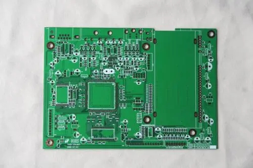
The full name of BGA is Ball Grid Array (PCB with ball grid array structure), which is a packaging method for integrated circuits using organic carrier boards. It has: less packaging area; increased functions and increased number of pins; self-centering when the PCB board is melted and easy to tin; high reliability; good electrical performance and low overall cost. PCB boards with BGA generally have many small holes. Most customers' BGA vias are designed with a finished hole diameter of 8-12mil. The distance between the surface of the BGA and the hole is 31.5mil as an example, generally not less than 10.5mil. BGA via holes need to be plugged, BGA pads are not allowed to be filled with ink, and BGA pads are not drilled.
The assembly of BGA devices is a basic physical connection process. In order to be able to determine and control the quality of such a process, it is required to understand and test the physical factors that affect its long-term reliability, such as the amount of solder, the positioning of wires and pads, and wettability, otherwise it is attempted to be based solely on electronics The results of the test are modified, which is worrying. The performance and assembly of BGA devices are superior to conventional components, but many manufacturers are still unwilling to invest in the ability to develop mass production of BGA devices. The main reason is that it is very difficult to test the solder joints of BGA devices, and it is not easy to guarantee its quality and reliability.
When BGA devices are assembled and produced using conventional SMT process procedures and equipment, they can consistently achieve a defect rate of less than 20 (PPM). Since the beginning of the 1990s, SMT technology has entered a mature stage. However, with the rapid development of electronic products in the direction of convenient/miniaturization, networking and multimedia, higher requirements have been put forward for electronic assembly technology. Density assembly technologies continue to emerge, among which BGA (Ball Grid Array package) is a high-density assembly technology that has entered the practical stage.