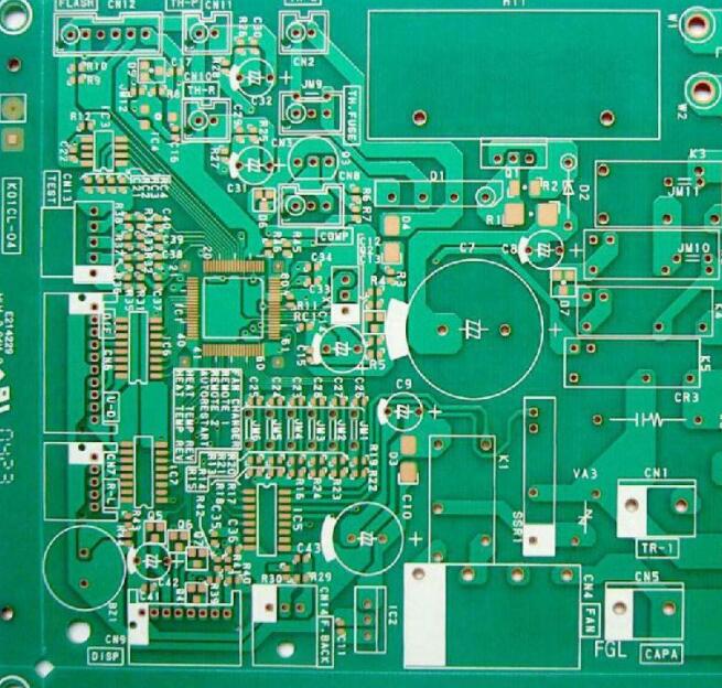
Most PCBA processing explosion cases are related to plate selection
PCBA foundry: the part of the sample of the burst board?
The partial appearance of the back of the failed sample (the other side corresponding to the light-colored part is a large device-electromagnetic relay)
After PCBA processing and reflow soldering, the sample bursting occurred after the lead-free reflow soldering. The failure sample bursting position was mainly distributed in the position of fewer devices and the large copper surface. After the slice analysis, it was found that the delaminated position of the bursting board was inside the paper layer. (image 3). Then the same batch of blank PCB boards were subjected to a thermal stress test at 260 degrees for 10 seconds, and only part of the board burst was found. Finally, we used TGA and DSC analysis techniques to analyze the glass transition temperature Tg and decomposition temperature Td of the sheet (see Figure 4). The results show that the Tg of the sheet is about 132 degrees, while the Td is only 246 degrees.
The slice photos of the PCBA foundry explosion area

Because the failure sample explosion position is mainly distributed in the position of fewer devices and the large copper surface, in the process of lead-free reflow soldering, due to the larger heat capacity, the location of the device is small, and the large copper surface absorbs more heat, which causes the sample to fail. The temperature is higher than elsewhere, and the darker color of the failure part also proves the above conclusion. The thermal decomposition temperature test results of PCBA processing materials show that the thermal decomposition temperature of the PCBA processing is 246.6 degree Celsius. Considering the lead-free reflow soldering process, the maximum soldering temperature is usually 245 degree Celsius~255 degree Celsius. Obviously, during the reflow soldering process The temperature of the paper layer cracking, the glass fiber layer, and the thermal decomposition temperature of PCBA processing are close to or even higher in the grinding direction of the large device with a small number of sample devices. When the soldering temperature exceeds the PCB thermal decomposition temperature, the PCBA processing will undergo thermal decomposition. Gas is generated, and the stress caused by gas expansion will cause the PCB to burst into delamination. Because the thermal decomposition temperature of the failed sample is close to the maximum welding temperature, a certain percentage of plate bursts fail.
PCBA partial blasting
A batch of PCBA samples has bubbles on the edge of a QFP device (see Figure 5), and the internal separation interface of the PCBA is between the copper foil and the PP layer. After a series of tests including thermal stress, glass state temperature analysis, decomposition temperature analysis and simulation process test, no similar phenomena and unqualified parameters were found. Finally, when using TMA to analyze the Z-axis coefficient of expansion (Z-CTE) of the material (Figure 6), it was found that the coefficient of expansion of the base material exceeded the standard range regardless of whether it was lower or higher than the Tg section.
The Z-CTE of the material itself is relatively high. During the lead-free reflow soldering process, the mismatch between the expansion coefficient of the resin and the metal copper foil (Z axis) causes the PCBA processing to expand due to heat, and the PCBA processing deformation during the subsequent cooling process Gradually recover, but at the lower end of the device, due to the restraint of the first solidified SOP solder joints, the PCBA processing under it cannot be recovered, and a large longitudinal stress is generated. When the longitudinal stress is greater than the adhesion between the copper foil and the resin At this time, it will cause the internal delamination of the PCB at this location. The soldering surface can be freely retracted due to the absence of the restriction of the QFP pins, so the failure mainly occurs at the interface between the core board resin and the copper foil near the QFP device surface. On the other hand, due to the distribution and structural characteristics of the pads and through holes at this location, the stress at this location is not easy to release, which makes this location more prone to failure of the board than other locations. Therefore, the design feature of the pad at this location is a factor that aggravates the board failure. factor.