How to meet the RF performance in the design of mobile phone circuit board without reducing the audio quality
Today, despite the ever-increasing audio functionality in mobile phones, much attention is still focused on the radio frequency subsystem in PCB board design, and audio circuits often receive the least attention. However, audio quality, especially with the characteristics of high-fidelity sound quality, has become one of the key points that affect whether a high-end mobile phone can quickly be accepted by the market. This article provides some suggestions to help ensure a well-layout circuit board without sacrificing audio quality.

A well-designed PCB boardmust be able to maximize the performance of each component mounted on it and avoid interference between different systems. Because if conflicts occur between the various subsystems, the result will inevitably lead to performance degradation. For PCB layout engineers, today's mobile phones present the ultimate challenge. Modern mobile phones include almost all the subsystems that can be found in portable devices, such as a variety of radio frequency modules (including cellular and short-range wireless transmission); audio and video subsystems; dedicated application processors; The I/O layout has been increased due to more and more application requirements, and each subsystem has conflicting requirements.
To integrate so many complex subsystems in such a small space, the actual situation to be considered is also all-encompassing. In addition to the possible interference between the same RF subsystems, the various subsystems may be caused by their own operation or wiring. Mutual interference, EMI problems, etc., all test the professional ability of mobile phone PCB engineers.
Recommended practice
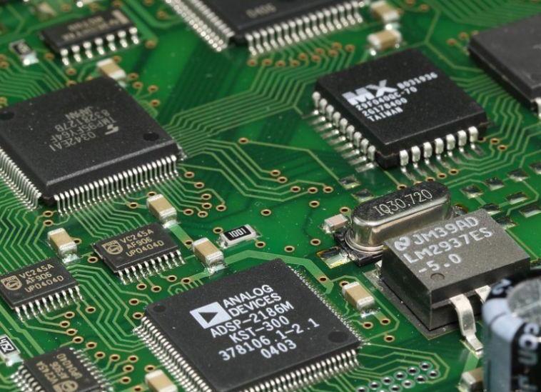
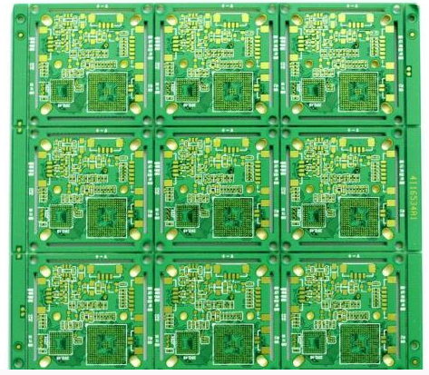
1. Carefully consider layout planning. The ideal layout plan should divide different types of circuits into different areas to minimize interference. The above picture shows a good layout plan.
2. Turn all unused areas on the circuit board into a ground plane. Ground flooding is performed near the signal traces, and the unwanted high-frequency energy in the signal line can be coupled to the ground through capacitors.
3. Isolate the ground current to avoid the digital current from increasing the noise of the analog circuit.
4. The analog circuit uses star grounding. The current consumption of audio power amplifiers is usually very large, which may have an adverse effect on their own ground or other reference grounds.
5. Use differential signals as much as possible. Audio components with differential inputs can suppress noise.
Not recommended practice
1. The analog audio signal wiring on the circuit board is too long. Analog audio traces that are too long may absorb noise from digital and RF circuits.
2. Use a hybrid circuit on the circuit board. Although the radio frequency area of a mobile phone is generally considered to be analog, the noise coupled from the radio frequency area into the audio circuit may be demodulated into audible noise.
3. Forget the importance of ground loops. Poorly grounded systems are likely to have serious distortion, noise, crosstalk, and low RF immunity.
4. Interrupt the natural loop of digital current. This path has the smallest loop area, which minimizes the effects of antenna and induction.