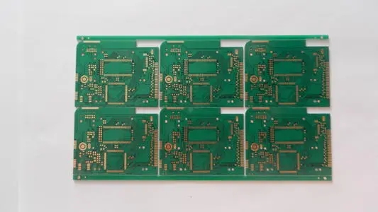
Introduce some suggested rules in PCB design

1. For discrete in-line devices
If the general resistance is discrete and in-line, the distance is slightly larger than the patch, which is generally between 1 and 3mm. Pay attention to keeping enough spacing (because of the trouble of processing, so the straight plug is basically not used)
2. We should pay attention to the minimum distance between the chip device (resistance and capacitance) and the chip and other devices. Chip: Generally we define the distance between the discrete device and the IC chip to be 0.5~0.7mm. Special places may change due to different fixture configurations.
3. Discrete devices near the edge
Since the PCB board is generally made of jigsaw, the devices near the edge need to meet two conditions. The first is to be parallel to the cutting direction (to make the stress of the device uniform), and the second is that the device cannot be placed within a certain distance ( Prevent damage to components when the board is cut)
4. For the placement of IC decoupling capacitors
A decoupling capacitor must be placed near the power port of each IC, and the location should be as close as possible to the power port of the IC. When a chip has multiple power ports, a decoupling capacitor must be placed on each port.
5. If the pad needs to consider the thermal pad in the paving area (must be able to carry enough current), if the lead is smaller than the pad of the in-line device, it needs to add teardrops (the angle is less than 45 degrees), which is also suitable for straight Plug the pins of the connector.
6. If adjacent pads need to be connected, first confirm that the connection is made outside to prevent bridging caused by the connection, and pay attention to the width of the copper wire at this time.
7. In addition, it should be noted that the lead should not be too close to the edge of the board, and it is not allowed to lay copper on the edge of the board (including the area near the positioning hole)
8. The width of the lead on both sides of the component pad should be the same. If there is a gap between the size of the pad and the electrode, pay attention to whether there will be a short circuit. Finally, pay attention to keep the pad of the unused pin and connect it to the ground or power supply correctly.
9. Note that it is best not to punch through holes on the pads.
10. Large capacitor: First, consider whether the ambient temperature of the capacitor meets the requirements, and secondly, keep the capacitor as far away as possible from the heating area.
To add a tragedy to the last point, we use patch capacitors and arrange them close to the heat source. During work, due to jitter and nearby heat, the solder joints of the capacitors are not sufficiently adhesive during work, which causes the capacitors to fall off. The tragedy happened, everyone must be cautious!
The above is the introduction of some basic rules in PCB design. Ipcb is also provided to PCB manufacturers and PCB manufacturing technology.