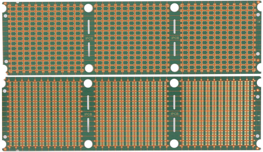
Compared with ordinary PCB boards in the design of multi-layer boards, in addition to adding the necessary signal wiring layers, the most important thing is to arrange independent power and ground layers (copper layers). In high-speed digital circuit systems, the advantages of using power and ground to replace the previous power and ground buses are mainly:
Provide a stable reference voltage for the conversion of digital signals.

Evenly apply power to each logic device at the same time
Effectively suppress crosstalk between signals
The reason is that the use of a large area of copper as the power supply and ground layer greatly reduces the resistance between the power supply and the ground, so that the voltage on the power layer is very uniform and stable, and it can ensure that each signal line has a close ground plane corresponding to it. At the same time, the characteristic impedance of the signal line is reduced, which is also very beneficial for effectively reducing crosstalk. Therefore, for some high-end high-speed PCB designs, it has been clearly stipulated that a 6-layer (or more) stacking solution must be used, such as Intel's requirements for PC133 memory module PCB boards. This is mainly considering the electrical characteristics of the multilayer board, as well as the suppression of electromagnetic radiation, and even the ability to resist physical and mechanical damage is significantly better than the low-layer PCB board.
If you consider the cost factor, it is not that the more layers the more expensive the price, because the cost of the PCB board is not only related to the number of layers, but also related to the density of the wiring per unit area. After reducing the number of layers, the wiring The space will inevitably be reduced, thereby increasing the density of the traces, and even the design requirements have to be reduced by reducing the line width and shortening the spacing. Often the cost increase caused by these may exceed the cost reduction by reducing the stack. Coupled with the deterioration of electrical performance, this approach is often counterproductive. Therefore, for designers, all aspects must be considered.