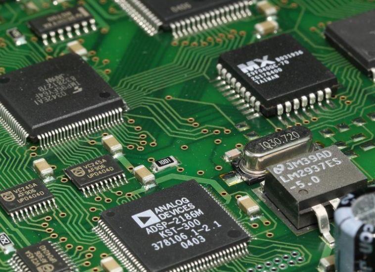
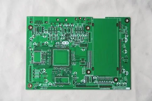
Of course it is based on the module. For example, what kind of chip is there, and then the peripheral circuits around it are put together, as well as the power supply part for the chip, the input and output terminals depend on your schematic diagram.

You have to know a little bit about circuits.
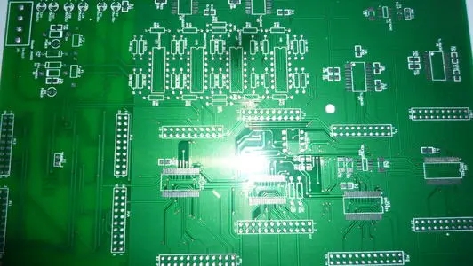
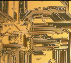
This must be divided into digital, analog, hybrid circuit, power supply, these must be divided in advance!
In addition to the special parts such as ESD, digital, analog, differential, high current and so on that need to be considered, the layout according to the schematic diagram is conducive to the layout of the circuit board.
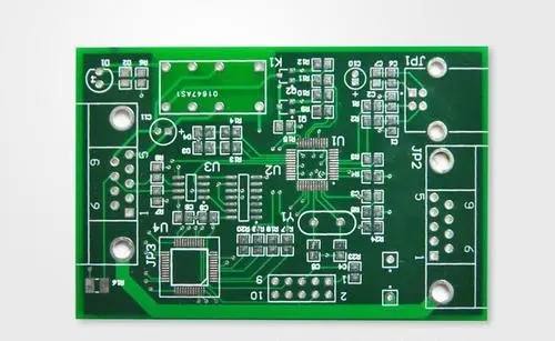
During the PCB layout process, after the system layout is completed, the PCB diagram should be reviewed to see whether the system layout is reasonable and whether the optimal effect can be achieved. It can usually be investigated from the following aspects:
1. Whether the system layout guarantees the reasonable or optimal wiring, whether it can guarantee the reliable operation of the wiring, and whether the reliability of the circuit operation can be guaranteed. In the layout, it is necessary to have an overall understanding and planning of the direction of the signal, as well as the power supply and ground wire network.
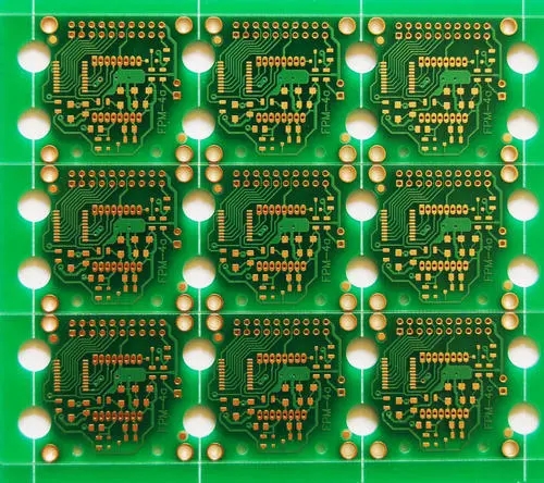
2. Whether the size of the printed board is consistent with the size of the processing drawing, whether it can meet the requirements of the PCB manufacturing process, and whether there is a behavior mark. This point requires special attention. The circuit layout and wiring of many PCB boards are designed very beautifully and reasonably, but the precise positioning of the positioning connector is neglected, resulting in the design of the circuit cannot be docked with other circuits.
3. Whether the components conflict in two-dimensional and three-dimensional space. Pay attention to the actual size of the device, especially the height of the device. When welding components that are free of layout, the height should generally not exceed 3mm.
4. Whether the layout of the components is dense and orderly, neatly arranged, and whether they are all laid out. In the layout of components, not only the direction of the signal, the type of signal, and the places that need attention or protection must be considered, but also the overall density of the device layout must be considered to achieve uniform density.
5. Whether the components that need to be replaced frequently can be easily replaced, and whether the plug-in board can be easily inserted into the equipment. The convenience and reliability of replacement and connection of frequently replaced components should be ensured.