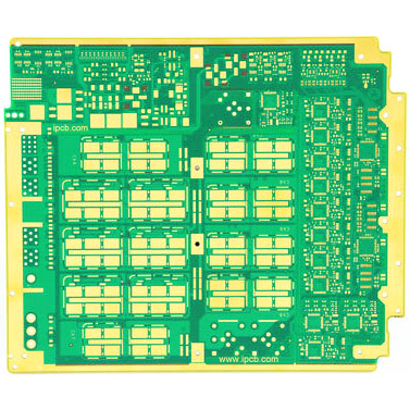
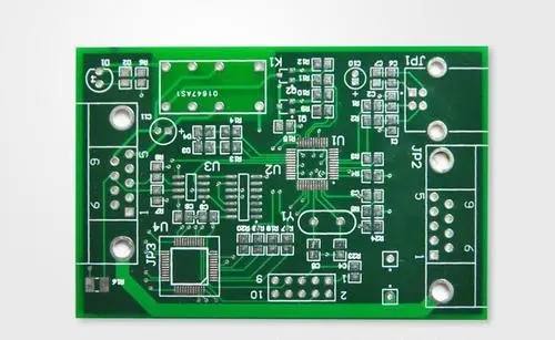
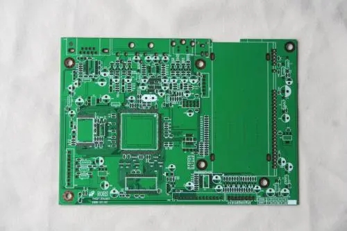
Precautions for PCB layout in switching power supply
1. Let me talk about the placement of Y capacitors first
The distance between the universal legs of the Y capacitor is 10mm, leave a pad, the middle gap is 8mm, and it is best not to run the wires in the middle
Do not route the wires in the middle, put them in the upper and lower boards, the left is strong current, the right is weak current, the strong current terminal GND is most suitable for power grounding, and the weak current terminal GND is best to be close to the GND pin of the transformer
For those who have the input ground wire, there is 3 Y, and the placement is also very delicate

The GND terminal of the Y-capacitor transformer is based on the design reference of "No Y-capacitor power supply", and I think the back capacitor is the same.
It is not difficult to see that the main current circuit in this picture should be the shortest, we can refer to it, it is more suitable for 5 to 40W power adapter
In addition to high power, please note the following two points:
1. It is best not to use jumpers in the main current circuit. If you must use jumpers, you need to add bushings. If the jumpers have components on the top, they need to be exempted.
2. In a limited flat area and within a safe distance as much as possible, if you are not bold, you need to add a secondary welding layer
3. Signal ground and power ground
Take PWM control anti-stimulation as an example. The difference between the two grounds is actually to protect the PWM chip from interference, that is, the chip needs auxiliary power, so the ground terminal of the chip should be connected to the auxiliary power filter capacitor instead of the large capacitance
For half bridge or full bridge, if the control chip is not isolated from the input, it is the same as anti-excitation. If isolated (for example, some have backup auxiliary power), you should add 1 to 3 0.1uF capacitors for the power supply.
4. Input LC filter
These switching power supplies are described here only for the wide voltage range of 85 to 264V
1. Enter the package size of the X capacitor. Because the size of the X capacitor has been standardized, if you need to add an X capacitor to the certification, if the package is small, it is a headache, so the X capacitor should be prepared at the beginning of the design, rather Make it bigger, not smaller. Save money and save other places. Don’t save it here.
2. The varistor, the sheath of the varistor is not a sheath, and the size of the sheath is larger, so like X capacitors, more space needs to be reserved.
3. L, common mode and differential mode, whether the design is differential mode or not needs to be verified, generally not for low power.
4. NTC / PTC, one is a negative temperature coefficient, the other is a positive temperature coefficient, both are to prevent inrush current.
1) When AC power enters the line, the minimum safety distance between the fuse and the two lines is not less than 6MM, and the minimum safety distance between the two lines and the chassis or internal ground is not less than 8MM.
2) Requirements for the rear line of the fuse: zero, and the minimum climb distance of the live line is not less than 3MM.
3) The minimum creepage distance between the high-voltage zone and the low-voltage zone is not less than 8MM, less than 8MM or equal to 8MM. The 2MM security slot must be opened.
4) The high-voltage area should have a silk-screen printed high-voltage warning sign, that is, a triangle sign with an exclamation point.
5) The minimum safety distance between the positive and negative filters of the high-voltage rectifier screen is not less than 2MM.
Therefore, the PCB factory should understand the precautions for PCB layout in the switching power supply, so that the PCB quality can be improved.