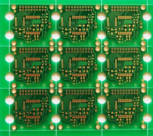
There are many discussions on the importance and layout principles of the ground wire in the literature, but there is still a lack of detailed and accurate introduction about the ground wire arrangement in the actual PCB board. My experience is that in order to improve the reliability of the system (not just make an experimental prototype), no matter how much emphasis is placed on the ground is not an exaggeration, especially in weak signal processing. To this end, we must spare no effort to implement the principle of "large area paving".

When paving the ground, it must generally be a grid-like ground, unless the scattered ground is divided by other lines. The thermal performance and high-frequency conductivity of the grid-like ground are much better than the whole ground wire. In double-panel wiring, sometimes in order to route the signal line, the ground line has to be separated, which is extremely disadvantageous for keeping the ground resistance low enough. For this reason, a series of "smart" methods must be adopted to ensure the "smoothness" of the ground current. These techniques include:
A large number of surface mount components are used to save the space occupied by solder holes that should belong to the ground wire.
Make full use of the front space: In the case of a large number of surface mount components, try to make the signal line go to the top layer as much as possible, and give the bottom layer "selflessly" to the ground. This involves countless small tricks, my own book "pcb" One of the design techniques: Switching Pins, there is a trick, and there are many similar spells, which will be written in the future.
Reasonably arrange the signal lines, and "give" important areas on the board, especially the "hinterland" (which is related to the communication of the entire board ground wire), to the ground wire. As long as it is carefully designed, this can still be achieved.
Coordination of the front and the back: Sometimes on one side of the board, the ground wire is really "destroyed". At this time, try to make the wiring on both sides coordinate with each other. At the corresponding position, leave a sufficient ground to lay the ground wire, and then pass through a sufficient number of vias with a reasonable location (considering that the vias have a large resistance), pass the signal line that will be crossed by the "bridge" The two sides of the Taiwan Strait that are forced to divide but are reluctant to part with the hope of reunification form a whole with sufficient conductivity.
The number of the dog jumping over the wall: When the huge ground wire is cut off by a small signal wire because I can't get out of the place, let the signal be wronged and use the jumper wire. Sometimes, I am unwilling to just pull a bare wire. This signal happens to pass through a resistor or other "long-leg" device. I can justifiably extend the pin of this device and make it serve as a jumper. It not only passes the signal, but also avoids the indecent name of the jumper wire:-(Of course, in most cases, I can always let such a signal pass through the appropriate place and avoid crossing the ground wire. The only thing needed is Observation and imagination.
The above is the introduction of ground wire layout experience in PCB design. Ipcb is also provided to PCB manufacturers and PCB manufacturing technology