1 Introduction
With the improvement of IC technology, processors from hundreds of megahertz to several gigahertz have become very popular. The past low-speed PCB designmethods can no longer meet the needs of increasing information development. The use of EDA tools to analyze and solve high-speed design The problem is an effective way. In the design process, the EDA tool analyzes the input device model data, and directly reports the results to the designer. The designer modifies and improves the design based on the feedback information. This shortens the development cycle and avoids waste of manpower and financial resources.

2 System composition
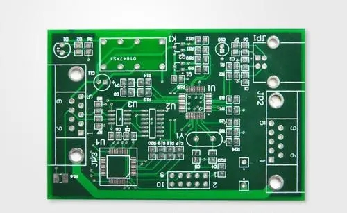
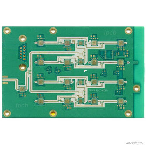
This test platform adopts MC9328MX1 in Motorola's Dragonball series chip, its CPU clock speed is 200MHz; SDRAM adopts SUMSUNG's synchronous K4S281632E, the clock speed is above 100MHz. Because the wiring density of the address bus and the data bus is relatively large, the speed is relatively high, and the system has high requirements for signal integrity, the PADS2004 design software of MENTOR is adopted, which integrates schematic design, PCB Layout and high-speed simulation analysis. It can solve the problems of signal integrity and crosstalk in PCB design, greatly improving the design success rate.
The most critical routing in the system is the connection routing between SDRAM and MC9328MX1. Their signal integrity directly affects whether the system can work normally. In PCB design, the PADS2004 software high-speed simulation tool HyperLynx is used for simulation. HyperLynx includes LineSim and BoardSim. LineSim is a simulation tool before wiring and BoardSim is a simulation tool after wiring. The simulation model adopts the IBIS model, and the IBIS model adopts the form of I/V and V/T tables to describe the characteristics of digital integrated circuit I/O units and pins. Since the IBIS model does not need to describe the internal design of the I/O unit and transistor manufacturing parameters, it is welcomed and supported by semiconductor manufacturers. Now major digital integrated circuit manufacturers can provide corresponding IBIS models while providing chips.
3 system design
3.1 Power distribution
The network distribution of the power layer in high-speed system board design is very important. In terms of PCB layout, the integrity of the power supply must first be considered on the PCB board, which directly affects the signal integrity of the final PCB board. In many cases, the main cause of signal distortion is the power system, such as poorly designed decoupling capacitors, unreasonable ground layer design, uneven current distribution, too much ground bounce noise, and serious loop effects.
Since the power supply layer distributes power through the entire metal layer, its power supply impedance is very small, so the power supply noise is much smaller than the bus type, so the power supply is used as a separate layer in the design.
In order to eliminate power noise, a 47uF capacitor is placed on the power input of the circuit board to eliminate low frequency noise. Place a 0.1uF high-frequency filter capacitor on the power pin and ground pin of each active device on the board to filter out the high-frequency noise of the line. The filter capacitor should be as close as possible to the power supply pin, and the wiring from the power supply pin to the filter capacitor should be the shortest to achieve the best filtering effect.
3.2 Clock design
Clock design is an important part of PCB design. By planning the clock line, make the connection of the clock line far away from other signal lines. The clock runs on the signal layer adjacent to the ground layer. Through multiple layers. The distance between the clock line and other data and address lines should meet the 3W principle (the spacing of the winding lines should be twice the line width). The clock connection should be as short as possible and ground protection should be added. In order to ensure the integrity of the clock signal, the output of the clock is connected in series with a terminating resistor of about 33 ohms.
3.3 Critical and non-critical signals
Before the simulation analysis, the signals in the system are divided into critical signals and non-critical signals. The principle of division is mainly based on conditions such as the driving edge rate of the device, the level of the operating frequency, and the length of the signal line. Of course, it should also be determined according to the actual design.
In this system, the key signals are: clock signal; CPU and SDRAM, CPU and FLASH and other memory data lines, address lines and read and write control signal lines. The most critical one is the connection routing between SDRAM and MC9328MX1. Their signal integrity directly affects whether MC9328MX1 can correctly access data in SDRAM.