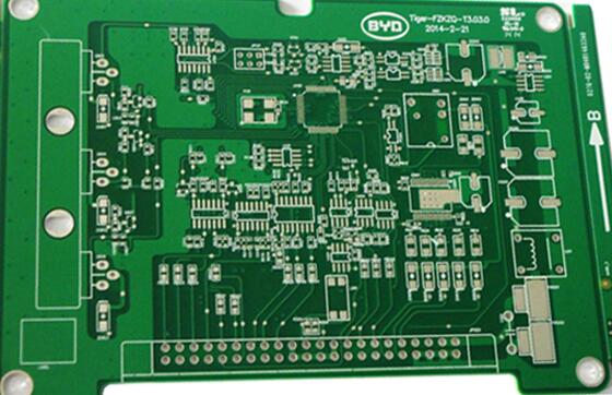
What are the common processing methods used by professional manufacturers for PCB proofing?
For companies engaged in PCB proofing and production and processing, the quality of the final PCB board is largely related to the surface treatment of the circuit board. If the professional circuit board manufacturer adopts the correct surface treatment method, It will greatly reduce the cost of the circuit board and improve the quality of the circuit board. If the wrong surface treatment is used, the circuit effect will not be fine enough, and it will also increase the cost of the PCB. So, in the current PCB proofing field, what are the surface treatment processes commonly used by circuit board manufacturers, and what are their respective characteristics?
PCB board
1. HASL hot air leveling process
This is the tin spraying method often referred to in the industry. This circuit board surface treatment method is the most commonly used treatment method in the early days of the industry. With the continuous changes of the times, it can now be divided into two different types: lead spray tin and lead-free tin spray The way, professional circuit board manufacturers can choose any way according to different circuit board surface treatment requirements and characteristics. Compared with other surface treatment methods of PCB proofing, the copper surface is completely wetted after the tin-sprayed PCB is completed, which is more conducive to the soldering of the circuit board, and also facilitates the progress of visual inspection and electrical testing.
2. Chemical nickel gold treatment process

This kind of PCB board proofing surface treatment process is a method with a wide range of applications. It is widely used in lead-free soldering processes and has strong resistance to environmental attacks. It is most common in switch contact design, electrical testing, SMT and aluminum wire bonding processes. . Professional circuit board manufacturers said that in the chemical nickel-gold surface treatment process, the nickel layer is a nickel-phosphorus alloy layer, and high-phosphorus nickel or medium-phosphorus nickel can be selected for different applications.
Circuit board
3. Nickel-palladium-gold treatment process
Compared with other circuit board surface treatment processes, nickel-palladium-gold has not been used for a long time in the field of PCB proofing, and this process has been widely used in previous semiconductor applications. The advantages of using the nickel-palladium-gold surface process for the circuit board are still very obvious. For example, it can be bound with gold wire and aluminum wire, and can be lead-free soldering. It can also be applied on IC carrier board, so it also has Low cost, corrosion resistance, compatible with a variety of surface treatment processes.
circuit board
4. Electroplating nickel gold treatment process
Among the many professional circuit board manufacturers at present, electroplated nickel gold is widely used in IC carrier boards, contact switch design, gold wire binding, and electrical testing. In specific processes, manufacturers often use hard gold or soft gold according to the difference in bonding connection design or whether additional conductive processes are needed.
Faced with various surface treatment methods of PCBA board proofing, professional circuit board manufacturers should choose the appropriate treatment method according to the actual situation and characteristics of the circuit board, and the budgeted cost.