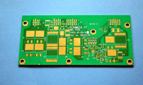
1. The PCB material currently used by MITAC
A. Urea cardboard
Features: The color is light yellow, often used for single-sided panels, but because it is made of urea paper, it is easy to rot in a cool and humid place, so it is not commonly used now.
B. CAM-3 board
Features: The color is milky white, the toughness is good, it has a high CTI (600V), and the carbon dioxide emission is only a quarter of the normal. It is now more commonly used in single-sided panels.
C. FR4 fiberboard
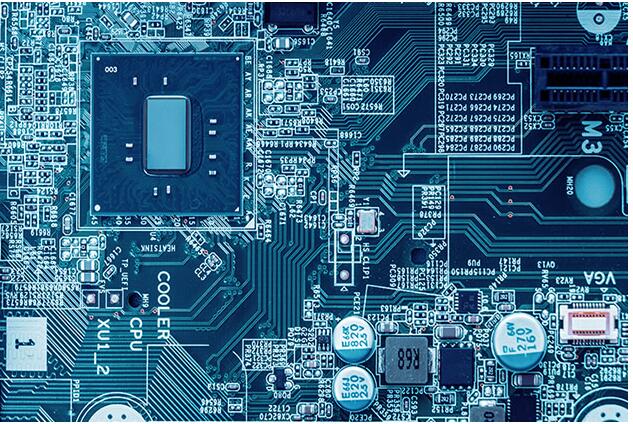
Characteristics: It is made of fiber, has good toughness, and when it breaks, there are wires pulling each other. It is often used for multiple panels. Its thermal expansion coefficient is 13 (16ppm/c). The mother board used by our factory is made of this board.
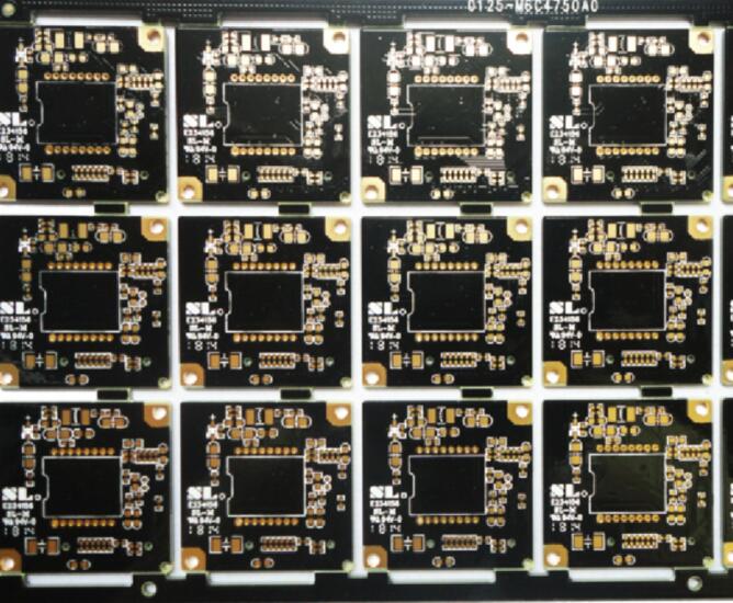
D. Multilayer board
Features: high Tg, high heat resistance and low thermal expansion rate, low dielectric constant and dielectric loss materials, mostly used for four or more layers.
E. Soft board
Features: The material is soft and transparent, it is often used in the electrical connection of two boards, and it is easy to fold. For example, the connection between the LCD and the computer body in a laptop computer.

F. Other
With a personal computer. With the popularity of multimedia digital information terminal products such as mobile phones, PCBs have become lighter, thinner, shorter, and smaller. Some large group companies abroad have successively developed more PCB boards, such as halogen-free, antimony-free environmentally friendly products, high heat resistance, high Tg boards, low thermal expansion coefficient, low dielectric constant, and low dielectric loss boards. Its representative products are: FR-5, Tg200 board, PEE board, PI board, CEL-475, etc. It’s just that it’s not popular in China yet.
2. The current MITAC PCB-Layout process
A﹒ R&D provides SCHMATIC (EE), FAB OUTLINE (ME) product development department provides us with schematic diagrams, and mechanical engineers provide us with peripheral information.
B﹒ Create new part
We call out the part from LIBRARIAN according to the schematic diagram. If there is no such part in LIBRARIAN, we will create a new part.
C﹒ Part layout
After the parts are ready, we need to lay out the parts
D﹒ ROUTING
This is our main task. After we set up the game, we will proceed to ROUTING.
E﹒ Final finishing
After ROUTING, we need to use FABLINK to finally sort out the various data we need
F﹒ Convert GERBER
Converted into GERBER documents required by PC board manufacturers
G﹒ Data save
After all the work is done, save the data for later modification and verification
three. Some basic terms about printing plates
On an insulating base material, according to a predetermined design, a printed circuit, a printed component or a conductive pattern formed by a combination of the two are made, which is called a printed circuit. On an insulating substrate, a conductive pattern that provides electrical connections between components is called a printed circuit. It does not include printing components. The finished boards of printed circuits or printed circuits are called printed circuit boards or printed circuit boards, also known as printed boards. Printed boards can be divided into two categories according to whether the substrate used is rigid or flexible: rigid printed board brushes and flexible printed boards. Rigid-flexible printed boards have also appeared this year. According to the number of layers of conductor patterns, they can be divided into single-sided, double-sided and multilayer printed boards. The entire outer surface of the conductor pattern is on the same plane as the surface of the substrate. The printing plate is called a flat printing plate.
After electronic equipment adopts printed boards, due to the consistency of similar printed boards, manual wiring errors can be avoided, and electronic components can be automatically inserted or mounted, automatic soldering, and automatic detection, ensuring the quality of electronic equipment and improving It improves labor productivity, reduces costs, and is easy to maintain. Printing boards have developed from single-layer to double-sided, multi-layer and flexible, and still maintain their respective development trends. Due to the continuous development of high precision, high density and high reliability The development of the direction, the continuous reduction of the volume and the reduction of the cost, make the printed board still maintain a strong vitality in the development of electronic equipment in the future.
4. V-1 grade FR-4?
FR-4 (flame-resistant laminated board) is based on "glass fiber cloth" as the main body, impregnated with liquid flame-resistant "epoxy resin" as a bonding agent to form a film, and then laminated to form boards of various thicknesses. The so-called V-1 refers to a sample of a copper-free glass fiber epoxy resin substrate with a width of 0.5 inches, a length of 5 inches and an arbitrary thickness. Measure the number of seconds for the flame to continue, and wait until the flame is completely extinguished before continuing to burn. After ten consecutive trial firings, those with a total delay of less than 250 seconds are called V-1 grade FR-4, and those with less than 50 seconds are called V-0 grade FR-4.
5. A brief history of PCB development
The basic concepts of printed circuits have been proposed in patents at the beginning of this century. In 1947, the American Aviation Administration and the American Bureau of Standards initiated the first technical seminar on printed circuits. At that time, 26 different printed circuit manufacturing methods were listed. It is classified into six categories: coating method, spraying method, chemical deposition method, vacuum evaporation method, molding method and powder compaction method. At that time, these methods failed to achieve large-scale industrial production. The adhesion problem of the pressure plate has been solved, the performance of the copper clad laminate is stable and reliable, and large-scale industrial production has been realized. The copper foil etching method has become the mainstream of the printed board manufacturing technology and has been developed to this day. In the 1960s, the hole metallization double Surface printing and multilayer printed boards have achieved mass production. Due to the rapid development of large-scale integrated circuits and electronic calculators in the 1970s, the rapid development of surface mount technology in the 1980s and multi-chip assembly technology in the 1990s promoted printing With the continuous advancement of circuit board production technology, a number of new materials, new equipment, and new testing instruments have emerged one after another. Printed circuit production technology has further developed in the direction of high density, thin wires, multilayer, high reliability, low cost, and automated continuous production. ﹒
6. Schematic design process
The generation of schematic diagram is generally regarded as the first step in the PCB production process. It is also the specific realization of the product vision by electronic engineering and technical personnel. ) Is composed of different logical connections. To make a schematic diagram, the source of its logical components is that some CAD software contains a huge logical component library (such as TANGO PADS, etc.), and some CAD software is in addition to logic
In addition to the library of logical components, users can also add new logical components (such as Cadence, Mentor, Zuken, etc.) by themselves, and users can use these logical components to implement the logical functions of the product to be designed.
1 Establish logic components
Logic components are components that provide a logic function (such as an LSOO gate, a flip-flop or an ASIC circuit).
1) The definition of the logical component model (or component name).
2) Package form of logic component pins
3) Description of logic component pins
4) Definition of the shape and symbol size of logical components
2 Functional description of logic components
To simulate the logic circuit, it is necessary to describe the functional characteristics of each logic component, such as the timing relationship of the logic component, the initial state rising edge (RISE), falling edge (FALL), delay time, and drive attenuation. Decay time, etc.
3 Description of the logic component library
Since there are many logic components, they are built under one library, which is easy to cause confusion and difficult to manage. Therefore, logic components with similar functional characteristics are generally placed under one library and managed according to functional characteristics, such as A/D, D/A conversion devices, CMOS devices, storage devices, TTL devices, linear devices, op amp devices, comparison devices, etc., are all placed in the same library. It can also be classified by company manufacturers such as: MOTOROLA, NEC, INTEL, etc.
.
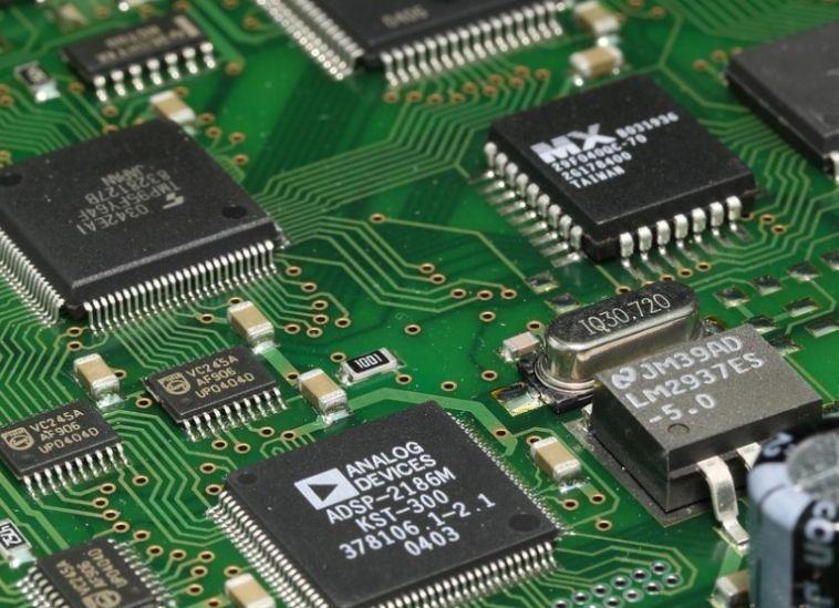
7. The function of printed circuit in electronic equipment
(1) Provide mechanical support for the fixing and assembly of various electronic components such as integrated circuits.
(2) Realize wiring and electrical connection or electrical insulation between various electronic components such as integrated circuits.
(3) Provide the required electrical characteristics, such as characteristic impedance, etc.
(4) Provide solder mask graphics for automatic soldering, and provide identifiers and graphics for component insertion, inspection, and maintenance.
8. In order to meet the requirements of environmental protection, how will PCB manufacturing technology change?
1) Reduce lead content
The method of using electroplated lead-tin to make pattern plating is tending to be quickly abolished. In the future, there will be more conversion to the entire panel plating (Panel Plating, also known as: Panel Plating) process method. In the case of using pattern electroplating production method, tin electroplating will also become the mainstream. In the case of using solder, the solder will be converted to a lead-free material, and there will be greater progress in this area in the future. It is expected that this change will have little impact on the entire PCB manufacturing process.
(2) Reduce the amount of formaldehyde used
Formaldehyde is used as a reducing agent for electroless copper plating (Electroless Copper Plating, also known as: electroless copper plating, electroless copper plating) in PCB production. At present, from the perspective of environmental protection, there will be stricter restrictions on its use in the future. In the future, through changes in the electroplating process, reducing or eliminating the use of formaldehyde materials will be the future development trend. Direct electroplating will become a widely used electroplating method. The re-understanding of the significance of the use of this electroplating method and the further improvement of this process are important tasks that need to be carried out in the future.
(3) Progress of MID
Thermoplastic resin is a polymer material that can be easily recycled. In order to meet the requirements of environmental protection and maintenance of the ecological environment in the future, thermoplastic resins will be used more in line circuit parts in the future. It is called: Molded Interconnect Device (MID), which will replace part of the traditional manufacturing technology PCB. MID will become a "new army" with development potential in PCB.
(4) Other materials
Solder resist materials, printed circuit board substrate materials (flame-retardant non-halogen-containing base materials) and other materials that are compatible with environmental protection will be developed and developed more and more quickly. This also makes the main materials used in the PCB manufacturing process change greatly. For this reason, in PCB manufacturing, the original process technology will be subject to considerable impact
9. High-speed circuit
It is generally believed that if the frequency of a digital logic circuit reaches or exceeds 45MHZ~50MHZ, and the circuit working above this frequency has taken up a certain share of the entire electronic system (for example, 1/3), it is called a high-speed circuit.
n fact, the harmonic frequency of the signal edge is higher than the frequency of the signal itself. It is the rising and falling edges of the signal (or signal jump) that cause unexpected results of signal transmission. Therefore, it is generally agreed that if the line propagation delay is greater than 1/2 of the rise time of the digital signal driving end, such signals are considered to be high-speed signals and produce transmission line effects. The transmission of the signal occurs at the instant when the signal state changes, such as the rise or fall time. The signal passes a fixed period of time from the driving end to the receiving end. If the transmission time is less than 1/2 of the rising or falling time, the reflected signal from the receiving end will reach the driving end before the signal changes state. Conversely, the reflected signal will reach the drive end after the signal changes state. If the reflected signal is strong, the superimposed waveform may change the logic state.
10. V_CUT
One way to shape the circuit board is to cut straight lines at the same position on the upper and lower sides of the board without cutting, so that it can be broken manually or using a jig to form a V-shaped groove from the top and bottom of the board, so it is called V_CUT
11.. Golden finger
it refers to some PCB circuit boards such as network cards. The gold-plated wires on the upper panel are called golden fingers because they are shaped like fingers.