Friends who are concerned about the development of the motherland's semiconductor industry may often see news about high-end lithography machines being stuck. Why are high-end lithography opportunities getting stuck? One of the reasons is the lens flatness of high-end lithography machines.

High-end EUV lithography machines have particularly high requirements for the flatness of the lens. It is said that if the area of a mirror is compared to the area of Germany, the surface roughness of the multilayer mirror provided by Zeiss can be controlled within 1mm above sea level. At present, only German Zeiss company can achieve this flatness. This is one of the reasons why we are stuck.
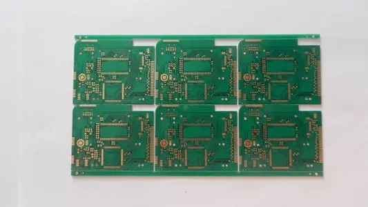
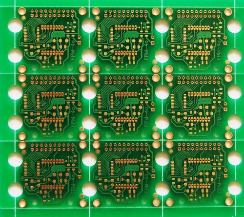
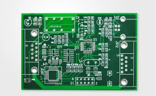
The lens of the lithography machine has flatness requirements, so the PCB circuit boards, which are various high-tech basic parts, also have flatness requirements. However, compared with the flatness of the lens of the high-end EUV lithography machine, the flatness requirement of the PCB board is far less high.
Let's take a look at the concept of PCB circuit board flatness and quality control issues.
The flatness of the PCB printed board is determined by two characteristics of the product: bow and twist.
The bowing state is determined by placing the four corners of the printed board on the same plane, roughly cylindrical or spherically curved.
Twisting is the deformation of the board parallel to the diagonal of the board, and one corner of the board is not on the same plane as the other three corners. Circular or oval printed boards must be evaluated for vertical displacement at the highest point. Bowing and twisting may be affected by PCB design, because different wiring or multilayer PCB structure may cause different stress or stress relief conditions. The thickness and material properties of the printed board are other factors that affect the flatness of the printed board.
Bow, twist or their combination shall be measured according to physical measurement methods and the percentage shall be calculated, in accordance with IPC-TM-650 test method 2.4.22, coordinate measuring machine (CMM) or equivalent method. The finished board should be evaluated according to the received state. For products made up for assembly, the bow and twist requirements should be determined by the PCB manufacturer through negotiation with the customer.
Acceptable conditions-level 3, 2, 1
• For PCB printed boards using surface mount components, bow and twist should be less than or equal to 0.75%.
• For all other printed boards, bow and twist should be 1.50% or less.
Not eligible-level 3, 2, 1
• The defect does not meet or exceed the above requirements.
Note 1 and Note 2: Deviation from the surface.
Note 3: Bow
Note 4: Force force is applied to two corners of the same side.