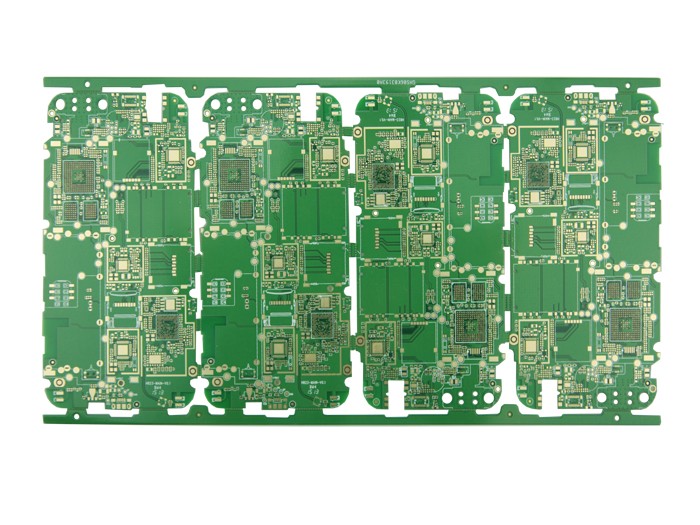
1. What PCB back drill?
Back drilling is actually a special kind of controlled depth drilling. In the production of multi-layer boards, such as the production of 12-layer boards, we need to connect the first layer to the 9th layer. Usually we drill through holes (one-time drilling), And then Chen Tong. In this way, the first floor is directly connected to the 12th floor. In fact, we only need the first floor to be connected to the 9th floor. Since the 10th to the 12th floor are not connected by wires, they are like a pillar. This column affects the signal path, which can cause signal integrity problems in the communication signal. So this extra pillar (called STUB in the industry) was drilled out from the reverse side (secondary drilling). So it is called back drill, but it is generally not as clean as the drill, because the subsequent process will electrolyze a little copper, and the drill tip itself is also sharp. Therefore, the PCB manufacturer will leave a small point. The length of this left STUB is called the B value, which is generally in the range of 50-150UM.

2. What are the advantages of back drilling?
1) Reduce noise interference;
2) Improve signal integrity;
3) Local plate thickness becomes smaller;
4) Reduce the use of buried blind holes and reduce the difficulty of PCB production.
3. What is the function of back drilling?
The role of back drilling is to drill out the through-hole sections that do not play any role in connection or transmission, to avoid reflection, scattering, delay, etc., which cause high-speed signal transmission, and to bring "distortion" to the signal. Research has shown that it affects the signal integrity of the signal system. The main factors include design, board materials, transmission lines, connectors, chip packaging and other factors, but the vias have a greater impact on signal integrity.
4. Working principle of back drilling production
Relying on the micro-current generated when the drill tip touches the copper foil of the substrate surface when the drill bit is drilled down to sense the height of the board surface, and then drill down according to the set drill depth, and stop the drill when it reaches the drill depth.
5. Back drill production process?
a. Provide a PCB with positioning holes on the PCB board, and use the positioning holes to drill and position the PCB and drill holes;
b. Electroplating the PCB after a drill hole, and dry film sealing the positioning holes before electroplating;
c. Make outer layer graphics on the electroplated PCB;
d. Perform pattern electroplating on the PCB after the outer layer pattern is formed, and perform dry film sealing treatment on the positioning holes before the pattern electroplating;
e. Use the positioning hole used by a drill for back drilling positioning, and use a drill to back drill the electroplated holes that need to be back drilled;
f. After back drilling, wash the back drilling with water to remove the residual drill chips in the back drilling.
6. If there is a hole in the circuit board, how to solve it from the 14th layer to the 12th layer?
1) If the board has a signal line on the 11th layer, there are through holes at both ends of the signal line to connect to the component surface and the solder surface, and the components will be inserted on the component surface, as shown in the figure below, that is, On this line, the signal is transmitted from component A to component B through the signal line on the 11th layer.
The above is an introduction to PCB back drilling technology. Ipcb is also provided to PCB manufacturers and PCB manufacturing technology