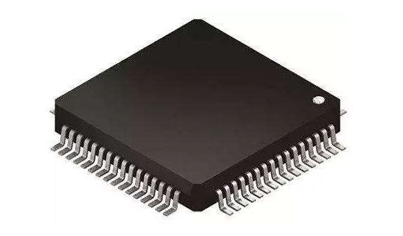
IC is the general name of semiconductor component products. IC can be divided into digital IC, analog IC, microwave IC and other ICs according to their functions.
Digital IC is the IC that transmits, processes and processes digital signals. It is the most widely used and fastest growing IC variety in recent years. It can be divided into general digital IC and special digital IC.
Analog ICs are ICs that process continuous natural analog signals such as light, sound, speed and temperature. Analog ICs can be divided into standard analog ICs and special application analog ICs according to their applications. If divided by technology, analog ICs can be divided into linear ICs that only process analog signals and hybrid ICs that simultaneously process analog and digital signals.
Standard analog IC includes amplifier, voltage regulation and reference comparison, signal interface, data conversion, comparator and other products; The special application analog IC is mainly used in four fields: communication, automobile, computer peripheral and consumer electronics.

Briefly summarize the differences between the two:
digital circuit IC is a device that processes digital signals, such as CPU, logic circuit, etc; The analog circuit IC is a device that processes and provides analog signals, such as operational amplifiers, linear regulators, reference voltage sources, etc. They are all analog ICs. The signals processed by analog IC are continuous and can be converted to sine wave for research, while those processed by digital IC are discontinuous signals, which are all pulse square waves.
Different digital devices have different manufacturing processes, so different power supply voltages are required, so the analog technology of power management is more needed. With the development of digital technology, analog technology is distributed around digital technology and is inseparable from digital technology. The comparison between digital technology and analog technology is as follows.
Let's explain the difference between analog IC and digital IC from the four characteristics of analog IC.
1. The life cycle can be as long as 10 years.
Digital IC emphasizes the ratio between operation speed and cost. The goal of digital IC design is to achieve the target operation speed at the lowest possible cost. Designers must constantly adopt more efficient algorithms to process digital signals, or use new processes to improve integration and reduce costs. Therefore, the life cycle of digital IC is very short, about 1-2 years.
Analog ICs emphasize high signal-to-noise ratio, low distortion, low power consumption, high reliability and stability. Once the product reaches the design goal, it will have long-term vitality. There are many analog IC products with a life cycle of more than 10 years. For example, the audio operational amplifier NE5532 is one of the most commonly used audio amplification ICs since it was introduced in the late 1970s. Almost 50% of multimedia speakers use NE5532, with a life cycle of more than 25 years. Because of the long life cycle, the price of analog IC is usually low.
2. Special process, less CMOS process
Digital ICs mostly use CMOS technology, while analog ICs rarely use CMOS technology. Because analog ICs usually need to output high voltage or high current to drive other components, while CMOS technology has poor driving ability. In addition, the key to analog ICs is low distortion and high signal-to-noise ratio, both of which are relatively easy to achieve under high voltage. CMOS technology is mainly used in low voltage environment below 5V, and continues to develop towards low voltage.
Therefore, analog ICs used Bipolar process in the early stage, but Bipolar process has high power consumption, so BiCMOS process appears again, combining the advantages of Bipolar process and CMOS process. In addition, there is CD process, which combines CMOS process with DMOS process. BCD process combines the advantages of Bipolar, CMOS and DMOS processes. In the high-frequency field, there are also SiGe and GaAS processes. These special processes need the cooperation of the wafer foundry and the familiarity of the designers, while digital IC designers basically do not need to consider the process issues.
3. Close relationship with components
Analog IC shall have good current amplification characteristics, small current characteristics, frequency characteristics, etc. in the whole linear working area; Due to the need of technical characteristics in design, it is often necessary to consider the symmetrical structure of component layout and the matching form of component parameters; Analog ICs must also have low noise and low distortion performance. Resistors, capacitors and inductors will generate noise or distortion, and designers must consider the impact of these components.
For digital circuits, there is no noise and distortion, and digital circuit designers do not need to consider these factors at all. In addition, due to the limitations of process technology, analog circuits should be designed with or without resistors and capacitors, especially high resistance resistors and large capacity capacitors, so as to improve integration and reduce costs.
The layout of some RF ICs on the PCB must also be considered, which is not considered in the digital IC design. Therefore, analog IC designers must be familiar with almost all electronic components.
4. Few auxiliary tools, long test cycle
Analog IC designers need both comprehensive knowledge and long-term experience. Analog IC designers need to be familiar with IC and wafer manufacturing processes and processes, as well as the electrical and physical characteristics of most components. Usually, few designers are familiar with the manufacturing process and flow of IC and wafer. In terms of experience, analog IC designers need at least 3-5 years of experience, and excellent analog IC designers need 10 years or more of experience.
There are few auxiliary tools for analog IC design, and the EDA tools that can be used are far less than digital IC design. Due to the large power consumption of analog IC and many factors involved, and the analog IC must maintain high stability, the authentication cycle is long. In addition, the test cycle of analog IC is long and complex.
Some analog IC products need to adopt special processes and packaging, and must be jointly developed with the wafer factory, such as BCD process and 30V high-voltage process. In addition, some products require WCPS wafer level packaging.