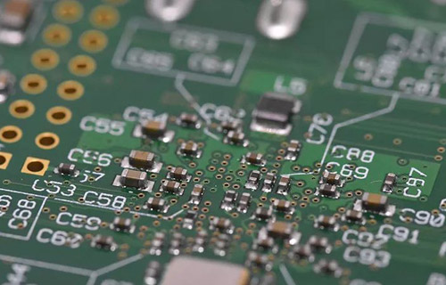
Common PCB board surface treatment processes include: OSP, electroless nickel plating/gold immersion, silver immersion, tin immersion, etc.
1. Silver immersion
The silver dipping process is between OSP and electroless nickel/gold dipping, which is simple and fast. Silver immersion does not wear thick armor on PCB. Even if exposed to heat, humidity and pollution, it can still provide good electrical performance and maintain good solderability, but it will lose luster. Because there is no nickel under the silver layer, silver immersion does not have all the good physical strength of electroless nickel plating/gold immersion. Silver immersion is a displacement reaction, which is almost submicron pure silver coating. Sometimes the silver leaching process also contains some organic substances, mainly to prevent silver corrosion and eliminate silver migration problems. Generally, it is difficult to measure this thin layer of organic substances, and the analysis shows that the weight of the organism is less than 1%.

2. Tin dipping
As all solders are based on tin, all tin layers can match any type of solder. From this point of view, the tin dipping process has great development prospects. However, tin whiskers are easy to appear in the previous PCB after tin dipping process, and tin whiskers and tin migration will bring reliability problems in the welding process, so the use of tin dipping process is limited. After that, an organic additive is added into the tin dipping solution to make the tin layer structure granular, which overcomes the previous problems and has good thermal stability and solderability. The tin dipping process can form a flat copper tin intermetallic compound, which makes the tin dipping have the same good solderability as the hot air leveling without the troublesome flatness problem of the hot air leveling; There is also no diffusion problem between electroless nickel plating and gold dipping metals; The tin dipping plate cannot be stored for too long,
3. OSP
OSP differs from other surface treatment processes in that it acts as a barrier between copper and air; To put it simply, OSP is to chemically grow an organic film on the clean bare copper surface. This film has oxidation resistance, heat shock resistance and moisture resistance to protect the copper surface from further rusting (oxidation or vulcanization, etc.) in normal environment; At the same time, it must be easily removed by the flux in the subsequent welding high temperature for welding. OSP is widely used in the industry due to its simple process and low cost. The early organic coating molecules are imidazole and benzotriazole, which play an anti rust role, and the latest molecule is mainly benzimidazole. In order to ensure that multiple reflow soldering can be carried out, only one layer of organic coating on the copper surface is not allowed. There must be many layers, which is why the chemical bath usually needs to add copper liquid. After coating the first layer, the coating layer adsorbs copper; Then the organic coating molecules of the second layer are combined with copper until the organic coating molecules of 20 or even 100 times are concentrated on the copper surface. The general process is degreasing -- micro etching -- pickling -- pure water cleaning -- organic coating -- cleaning. Compared with other processes, process control shows that the treatment process is relatively easy.
4. Chemical gold
Gold deposition and gold plating are commonly used in PCB proofing, and many people cannot correctly distinguish between them. Electroplated nickel gold generally refers to "electroplated gold", "electrolytic gold", "electroplated gold" and "electroplated nickel gold plate". It makes gold particles adhere to PCB board through electroplating. It is called hard gold because of its strong adhesion; The process can greatly improve the hardness and wear resistance of PCB, effectively prevent the diffusion of copper and other metals, and meet the requirements of hot pressing welding and brazing. The coating is uniform and fine, with low porosity, low stress and good ductility. Therefore, it is widely used in PCB proofing of electronic products. Then what is sinking gold? Gold deposition refers to the chemical reaction and the crystallization of gold particles, which are attached to the bonding pad of PCB board. Because of the weak adhesion, it is also called soft gold. Electroless nickel plating/gold dipping is to wrap a thick layer of nickel gold alloy with good electrical properties on the copper surface and can protect PCB boards for a long time. Unlike OSP, which is only used as a rust proof barrier, it can be useful in the long-term use of PCB boards and achieve good electrical performance. In addition, it also has the environmental tolerance that other surface treatment processes do not have. The reason for nickel plating is that gold and copper will diffuse each other, and the nickel layer can prevent the diffusion between them. If there is no barrier of nickel layer, gold will diffuse to copper in a few hours. Another advantage of electroless nickel plating/gold leaching is the strength of nickel. Only 5um thick nickel can control the expansion in Z direction at high temperature. In addition, electroless nickel plating/gold immersion can also prevent the dissolution of copper, which will be beneficial to lead-free welding. The general process is: deacidification cleaning -- micro etching -- pre leaching -- activation -- chemical nickel plating -- chemical gold leaching; There are 6 chemical tanks in the process, involving nearly 100 kinds of chemicals, and the process is relatively complex.
Main differences between PCB board gilt plate and gilded plate:
1) The thickness is different. Because the crystal structures formed by the two are different, in general, the thickness of gold deposited is much thicker than that of gold plating. Therefore, golden yellow is more common in gold deposition, and the yellower is gold plating.
2) Because the crystal structure formed by gold plating is different from that formed by nickel gold plating, gold plating is easier to weld than gold plating. At the same time, because gold plating is softer than gold plating, gold finger plates generally choose nickel gold plating because hard gold is wear-resistant.
3) With different crystal structures, the crystal structures formed by gold deposition and electroplated nickel gold are different, and gold deposition is relatively easier to weld,
4) In the PCB proofing process, nickel gold electroplating and gold precipitation belong to the surface treatment process. The difference is that nickel gold electroplating is done before resistance welding; And gold deposition is done after resistance welding on PCB board.