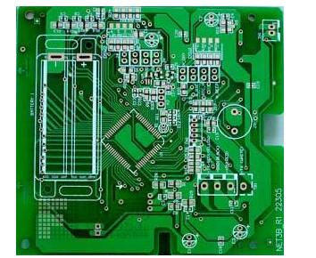
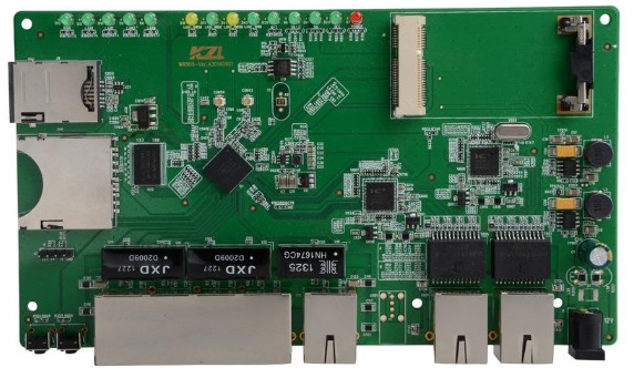
What are the requirements for PCBA processing and welding? During the soldering process, the soldering iron tip should be frequently scrubbed to avoid dirt or other impurities on the soldering iron tip from affecting the finish of the soldering joint. When cutting the feet after soldering, use diagonal pliers,PCBA patch processing and cutting pliers can not be close to the circuit board, about 2MM away from the circuit board, to prevent the solder joints from being cut, only cut off the excess ends. The horizontal components on the PCBA board must be affixed to the PCBA board, and the vertical components must be affixed and inserted on the PCBA board vertically, and there should be no swaying of the components and the unplugging of the components. When the PCBA board is immersed in tin, the tin points should be fully and smoothly immersed, and there should be no undesirable phenomena such as submerged tin and dissatisfaction with the tin point immersion.
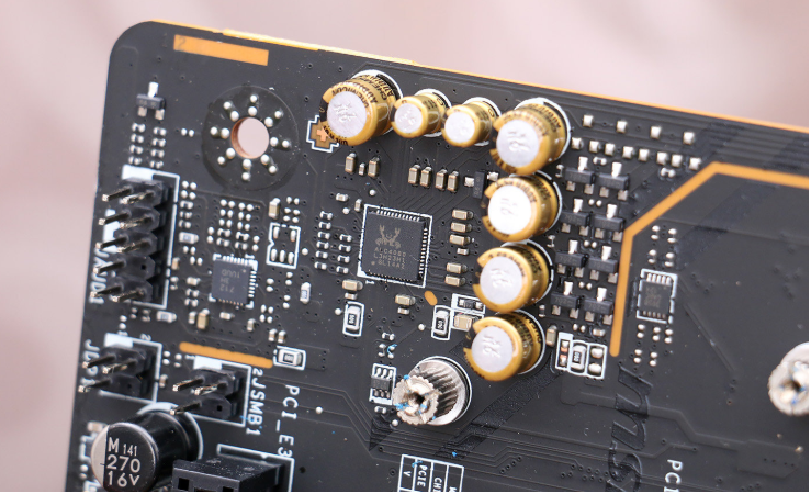
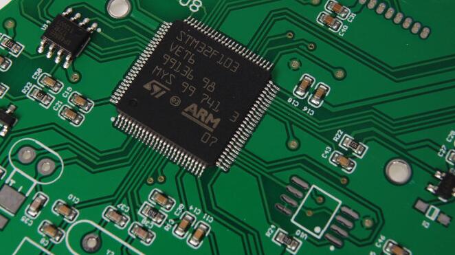
When soldering the solder joints on the PCBA board, do not use too much tin, otherwise the solder joints will be too large and swollen. At the same time, the solder joints should be smooth and free of shuttle corners, chamfers and gaps. The smt process will be welded at the same time. Spot welding must be firm, and there should be no undesirable phenomena such as cracking of tin. The components on the PCBA board must not have any defects such as missing parts, reversed component insertion, and wrong component insertion. When plugging in components on the PCBA board, one side cannot be high and the other low, or both sides are much higher at the same time. Wear an anti-static wristband when soldering the IC. One end of the electrostatic wristband should be well grounded to prevent damage to the IC. The PCBA board must not have undesirable phenomena such as desoldering, oxidation, loose pads, copper skin lifting, open circuit, virtual soldering, short circuit and so on. The finished PCBA board must be cleaned with rosin and other impurities on the board with washing water or alcohol. There should not be any food or drink in the PCBA work area, smoking is prohibited, no sundries that are not related to work should be placed, and the circuit board processing should keep the workbench clean and tidy.

Regularly check EOS/ESD workbenches to confirm that they can work normally (anti-static). The various dangers of EOS/ESD components can be caused by incorrect grounding methods or oxides in the ground connection parts. Therefore, special protection should be given to the "third line" grounding terminal joints. It is forbidden to stack PCBA. Physical damage will occur in the processing of circuit boards. Special brackets should be provided on the assembly work surface, and they should be placed according to their types. During PCBA patch processing, the welded surface should not be taken with bare hands or fingers, because the grease secreted by human hands will reduce the weldability and easily lead to welding defects. The operation steps of PCBA and components are reduced to a minimum, PCBA can prevent danger. In assembly areas where gloves must be used, soiled gloves will cause contamination, so gloves must be replaced frequently when necessary. Do not use skin-protecting oils to coat hands or various silicone-containing detergents, as they can cause problems in solderability and adhesion of conformal coatings. A specially formulated detergent for PCBA soldering surface is available. In PCBA patch processing, these operating rules should be strictly followed, and the correct operation of electronic processing can ensure the final use quality of the product, and reduce the damage of components and reduce the cost. Components and PCBA that are sensitive to EOS/ESD must be marked with appropriate EOS/ESD marks to avoid confusion with other components. In addition, in order to prevent ESD and EOS from endangering sensitive components, all operations, assembly and testing must be completed on a workbench that can control static electricity.