PCBA proofing on-site follow-up questions: how to prevent errors in SMT patch processing
PCBA sales staff generally have a lot of contact with customers and have a certain understanding of SMT and PCBA processing procedures, but they may not have a deep understanding of the problems in the actual production process. At the request of individual customers, the business personnel of Shenzhen Youqin Electronics are required to follow up a PCBA proofing on site. The company also requires a summary report to reflect the possible and frequently encountered problems in PCBA proofing. This article is from the customer's point of view. How to follow up the production line, and if you control the SMT processing and key links, avoid serious errors such as leaking, wrong, and reversed electronic components.
Follow up with two BOM PCBA proofs, one is pure plug-in, the other is single-sided mixed assembly (single-sided both patch and plug-in), because each proofing 10 pieces, the plug-in is changed to manual welding. First of all, make preparations and print out the tag numbers of the BOM, patch and plug-in. Mark the key inspection items on the BOM, mainly marking the components with polarity such as diodes, electrolytic capacitors, ICs, etc.
When I came to the plug-in workshop, a plug-in board was already welded. At first glance, it feels the same as looking at the BOM, this board is very simple! But the welding supervisor responded to two problems: the LED light must control the height and the distance between the front, rear, left, and right, and it must be able to accurately cut into the lamp hole of the housing after welding, which is very difficult to solder; the second problem is the capacitor foot pitch at the C4 position and the PCB. The disagreement. The distance between the pins on the PCB board is too large, and the batch needs to be modified according to the actual distance of the capacitor.

Compared with the welding supervisor's statement that LED lights are difficult to weld, a careful study found that one must control the height of the LED lights, and at the same time, ensure that each LED light can be accurately cut into the LED light hole of the plastic shell after it is welded. It is easy to solder one lamp. It is really a challenging technical task to solder a total of 16 lamps in two rows to ensure the accuracy of the height and the front, rear, left, and right distances. A solution must be found during mass production. Combine the picture above, look at the picture below, and try to figure it out. It is not easy to solder these 23 lights.
Now that the welding is done, let's be the first article inspector directly. Check the polarity of solder joints and components. There are 23 plug-in LEDs on this board, an IC and an electrolytic capacitor are polarized. The solder joints are good, and the appearance is not bad. The electrolytic capacitor and the component identification of the IC and the silk-screen identification of the PCB are matched, and there is no problem with the polarity. However, there seems to be something wrong with the LED.
Generally speaking, the long leg of the LED lamp should be the positive pole, or the side with more metal in the lamp body should be the negative pole. However, comparing the silk screen on the PCB board and the identification of the components, it turns out that there is a problem. Please take out the multimeter and measure it. As expected, the soldering staff accidentally soldered the LED lights upside down. No need to say, rework, remove the LEDs and re-solder!
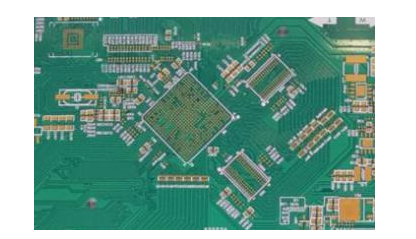
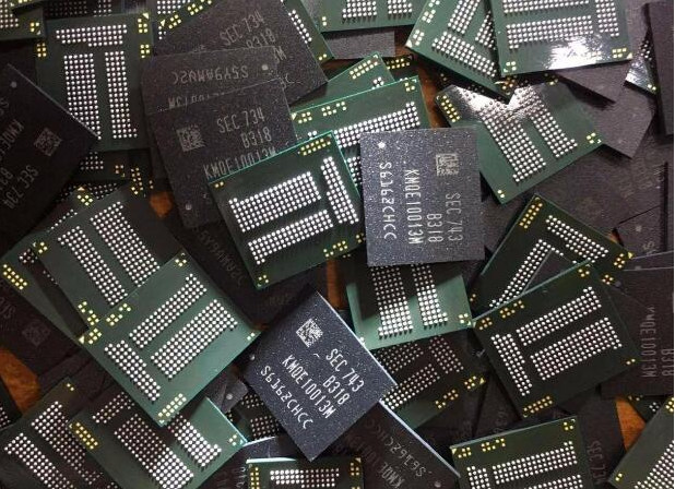
When I came to the SMT workshop, the proofing staff complained to me. There were 10 sets of proofing, but only 11 sets of capacitors and resistors were supplied. I said that this must be a problem with the customer’s work and must be improved next time, but this time, be careful. I believe that the master's superb technique will definitely be able to do nothing. People like to listen to good words, doing things is efficient, the proofing master really controls it well, and SMT patches have posted 10 sets of boards. In the first inspection, the staff raised a question against the LED light at D4 position. The polarity of the PCB silkscreen at D4 position is contradictory: the negative electrode is expressed in the direction of a regular triangle, but the side with a vertical line is also negative. For this figure, these two points are in contradiction.
This problem should have been discovered before it went online, and now it is discovered that it is "it is not too late to make up for it." I immediately called the customer's engineer. The engineer checked the design and confirmed that there was a contradiction. Here, the direction of the power arrow shall prevail, and he also praised us for the careful and meticulous work of Uqin Electronics. I was in a good mood to be praised, and the other 9 boards were posted in one go. I took three boards and carefully compared the BOM and polar components to check for missing components, reversed components, and solder joints. Generally speaking, it felt good within the visible range of the naked eye.
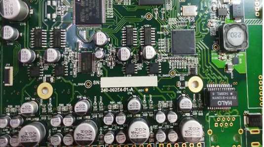
At the same time as the visual inspection, the AOI also began to inspect. For the proofing PCBA, Shenzhen Youqin Electronics Co., Ltd. strictly requires the first inspection and AOI inspection. Of course, the SPI inspection after solder paste printing is also necessary. However, many companies in the industry do only visual inspection to save time when making prototypes. They do not do first piece inspection and AOI inspection. For a more complex PCBA, the quality is actually difficult to guarantee. At the same time of AOI inspection, I also called PMC to quickly coordinate and arrange manual hand welding directly after inspection. While the DIP department was welding, the first plug-in model was carefully checked. The second PCBA is soldered like this:
From the customer's point of view, on-site follow-up PCBA proofing summary:
1. The PCBA processing plant must have first-piece inspection and AOI inspection for samples, and see the strict implementation of these two procedures on site;
2. If necessary, the customer must hold a pre-production meeting with the PCBA processing plant to pay attention to the technical difficulties of the problems and how to control them during the processing;
3. Make preparations for follow-up: Print the PCB silkscreen bit number map, BOM table, mark the components with polarity, and have an overall understanding of the PCBA products to follow.
4. Focus on inspecting the quality of solder joints, whether the components are missing, incorrectly pasted, and reversed. You can randomly select 3-5 identical PCBAs and place them on the same side and in the same direction to see if the components are different, whether the polarity of the IC and the electrolytic capacitor are correct and consistent. LED lights can be used to test two or three boards with a multimeter to ensure that there are no appearance problems, quality problems such as leaking, wrong and reverse pasting;
5. Problems that are not convenient for mass production should be reported back to customers in time, such as PCB silk screen, changes in the pitch of some components, etc. Proofing is to find problems in production. If there is any improvement, whether it is a PCBA processing plant or a subtle PCB modification, it must be improved.