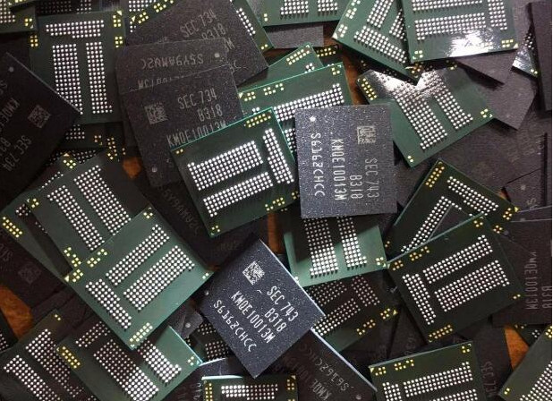
Under what circumstances will PCBA boards and PCB boards suffer from electrostatic damage, it can be said that the entire process of electronic products from production to use is threatened by electrostatic damage, from device manufacturing to dip plug-in assembly and welding, complete machine assembly, packaging and transportation until Product applications are under the threat of static electricity.
In the entire production process of electronic products in the PCB factory, at every small step in every stage, electrostatic sensitive components may be affected or damaged by static electricity. In fact, the most important and easily neglected point is the transmission of components. During this process, the transportation is easily exposed to the external electric field (such as passing near high-voltage equipment, workers moving frequently, vehicles moving quickly, etc.) resulting in static electricity and being damaged. Therefore, special attention must be paid to the transportation and transportation process. Reduce losses, avoid indifferent disputes, and add Zener voltage regulator protection if you protect it.

First, the input resistance of the MOS tube itself is very high, and the capacitance between the gate and the source is very small, so the PCB board and PCBA board are very susceptible to the external electromagnetic field or electrostatic induction and charged, and a small amount of charge can be on the capacitance between the electrodes. A relatively high voltage (U=Q/C) is formed, which will damage the tube. Although the MOS input terminal has anti-static protection measures, it still needs to be treated with care. It is best to use metal containers or conductive materials for storage and transportation. Put it in chemical materials or chemical fiber fabrics that are prone to static high voltage.
Second, the protection diode at the input end of the MOS circuit generally has a current tolerance of 1mA when it is turned on. When the PCB circuit board may have excessive transient input current (over 10mA), the input protection resistor should be connected in series, so it can be used in application. Choose a MOS tube with a protective resistance inside, and because the instantaneous energy absorbed by the protective circuit is limited, too large instantaneous signals and excessive electrostatic voltage will make the protective circuit useless, so the electric soldering iron must be reliably grounded during welding. The input terminal of the device to prevent leakage and breakdown. In general use, the residual heat of the electric soldering iron can be used for soldering after the power is turned off, and the grounding pin should be soldered first.
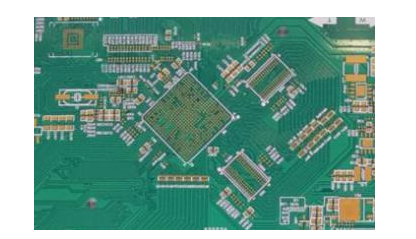
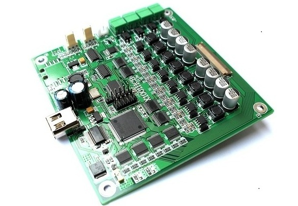
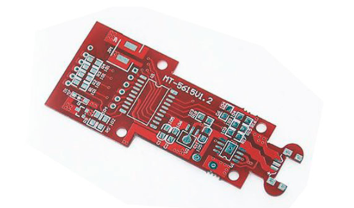
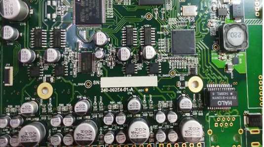
Desoldering technology in PCBA processing. The main points of the work that the chip factory can desolder:.
(1) Strictly control the heating temperature and time to avoid high temperature damage to other components. Generally, the time and temperature of desoldering are longer than those of soldering.
(2) Do not use too much force during desoldering. The package strength of components under high temperature will decrease. Excessive pulling, twisting, and torsion will damage components and pads.
(3) Absorb the solder on the desoldering joints, you can use the suction tool to suck the solder, and the components are directly unplugged, reducing the desoldering time and the possibility of damaging the PCB.