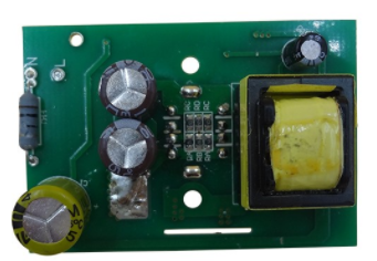
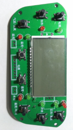
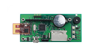
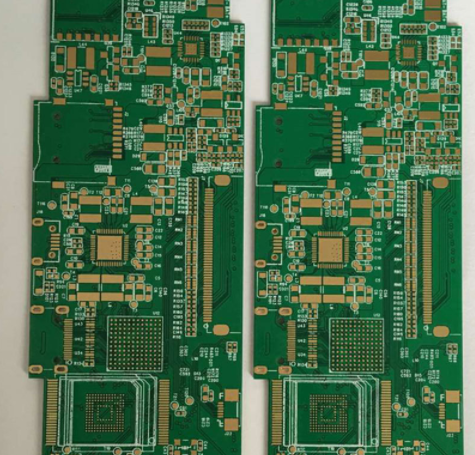
The application of ball implantation technology in SMT chip processing industry is becoming more and more necessary, and EMS companies can only respond to the requirements of OEM customers if they have mastered wafer-level and chip-level packaging technologies. The following is an introduction to the ball planting technology applied on the PCBA circuit board.
The whole process includes four steps: coating flux, planting balls, inspection and rework, and reflow soldering. Two online printers are required for ball planting: one is an ordinary screen printer for applying paste flux, and the other is for ball planting. Both printing presses can be switched to ordinary printing presses for electronic assembly at any time. Coating Flux Coating paste flux is the first step of the ball planting process. It is a key step to maintain the positioning of the ball and to form a good shape in reflow soldering. A specially designed screen is used for the printing of paste flux. The opening of the screen is determined based on the size of the printed circuit board and the size of the solder balls. In the step of printing paste flux,

two types of squeegees are used at the same time, and the front squeegee is a rubber squeegee. The vertical squeegee first coats a thin layer of flux evenly on the screen, and then the rubber squeegee prints the flux on the PCBA circuit board pads. DOE is used to determine the best parameters for flux printing. After SMT chip processing is printed, observe and calculate the coverage of flux on the pad with a microscope, and calculate the result of DOE. The flux coverage reflects the results of the DOE experiment.
In this DOE experiment, the most optimized printing parameter settings can be obtained; of course, different equipment will have certain differences. In the SMT patch processing and production process, the stencil is easily damaged, so it needs to be handled and moved carefully. In the process of flux printing, solid dust or other foreign substances can easily block the opening of the screen, which can only be cleaned with an air gun. Cleaning agents such as isopropyl alcohol or alcohol can not be used to clean the screen, because it will dissolve and destroy the polymer material on the screen. Usually, after the production is finished, wipe it with a dust-free cloth dampened with deionized water and dry it with an air gun. After the flux printing of SMT patch processing is completed, it is necessary to check under a microscope for insufficient or misaligned print. Usually the flux is transparent, and it is difficult to detect defects by visual inspection. In the ball planting stage, a specially designed template is also required.
The opening design of the template is also based on the actual solder ball size and PCB circuit board pad size. This is based on two considerations: one is to prevent the flux from contaminating the template and the solder balls; the other is how to make the solder balls pass smoothly Template opening. The template structure has two layers: the main body is an electroformed template, which has a smoother hole wall than a laser or chemical etching template, so that the solder ball can pass smoothly; the composite two layers have almost the same thickness as the diameter of the solder ball, which is very good Therefore, the contamination of the electroforming template by the paste flux is avoided, and at the same time, the solder balls can smoothly pass through the template to reach the pad and be stuck by the flux. AOI equipment is used for on-line inspection after ball planting in SMT patch processing. The main defects are usually fewer balls and misalignment. After the inspection, the circuit board with fewer balls needs to be reworked with offline semi-automatic ball filling equipment; for misalignment defects, cleaning the PCB circuit board and reprinting is the only way. The placement of fewer balls requires the use of an accurate image magnification system. First, an operating arm is used to apply paste flux on the ball-missing pad, and then another operating arm is used to fill the ball on the pad. For lead-free products, the generally used solder alloy is SAC105, which has a slightly higher melting point than the lead-free solder paste used for PCB circuit boards to prevent defects from being caused again in the secondary reflow. AOI inspection is required after reflow soldering.