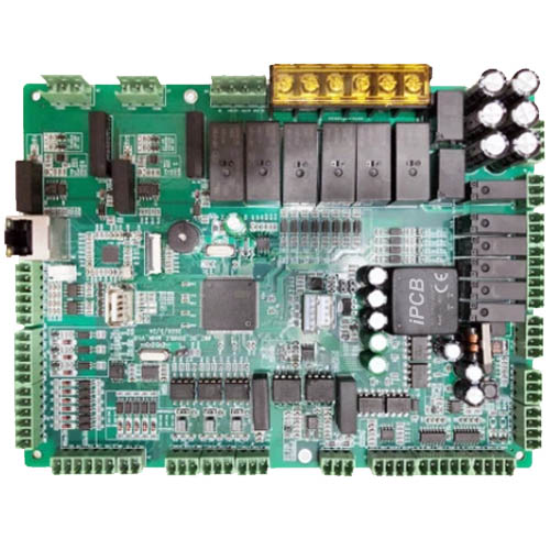
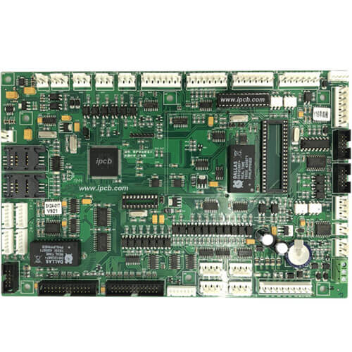
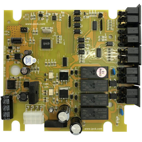
FPGA multi data acquisition card PCBA
Layers : 12Layers
Surface Process : Immersion Gold
Gold thickness : 2U
PCB Color : Green solder mask
PCB Testing : Yes
PCBA Testing : Yes
Provide PCB Manufacturing : Yes
iPcb company provide full electronic components.
PCBA Testing : Yes ( Customer provide testing step with video )
RoHS compliant lead-free assembly
Advantages of FPGA multi data acquisition card PCBA
Because of its high clock frequency, small internal delay, high speed, high efficiency and flexible composition, FPGA has incomparable advantages in high-speed data acquisition between DSP and MCU.
The data acquisition system of FPGA multi data acquisition card adopts modularized design structure, which is composed of 4 modules. Each acquisition module can be interchanged or flexibly increased. The modules are connected by three way connectors. The sensor signals and 422 serial signals are input to the corresponding module, and the main control module controls the unified framing and transfers to the double backup memory. The design scheme is flexible and easy to control, which has good practical value.

Advantages of FPGA multi data acquisition card PCBA
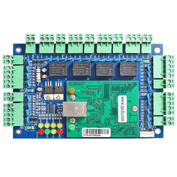
System PCBA hardware design
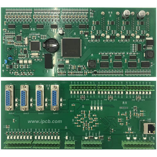
The data acquisition and recording system is composed of one main control card and three data acquisition cards. The main control card is the core part of the data acquisition system, which mainly includes long-line communication of ground measurement and control station, data transmission control of each data acquisition card, data forwarding, memory control and other functions. The three data acquisition cards can collect 72 analog signals. The FPGA in each data acquisition card controls the multi-channel switch from the control module according to the address jumper module. One of the 24 analog signals is selected and converted into digital signal by 16 bit a / D converter. After the signal acquisition of each channel is completed, the collected data is passed through the three-way stackable internal total according to the receiving sequence and handshake signal The data is transmitted to the main control card, and then the frame is unified by the FPGA main control module of the main control card, and then transmitted to the memory to complete the data acquisition and storage process.
The switching of multi-channel analog switch is an important content of data acquisition card. In this design, each data acquisition card needs to collect 24 analog signals with different frequencies at the same time, so it is necessary to control the switching and selection of sampling channel address with high precision and accuracy, which puts forward high requirements for the design of hardware and software. The analog switch used in the hardware part is adg706, which is a chip that can select 16 channels of signals. Since the acquisition channel is 24 channels, each acquisition card needs two adg706 chips, and the switching value reaches 16x2 = 32 > 24 channels, which meets the PCB design requirements.
FPGA multi data acquisition card PCBA
Layers : 12Layers
Surface Process : Immersion Gold
Gold thickness : 2U
PCB Color : Green solder mask
PCB Testing : Yes
PCBA Testing : Yes
Provide PCB Manufacturing : Yes
iPcb company provide full electronic components.
PCBA Testing : Yes ( Customer provide testing step with video )
RoHS compliant lead-free assembly
For PCB technical problems, iPCB knowledgeable support team is here to help you with every step. You can also request PCB quotation here. Please contact E-mail sales@ipcb.com
We will respond very quickly.