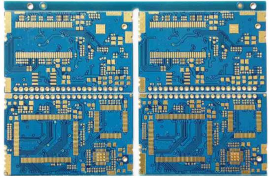
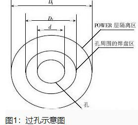
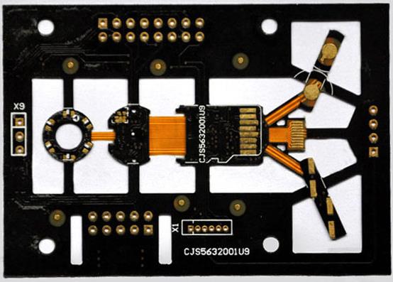
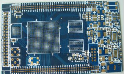
PCB vias are holes on printed circuit boards used for electrical connections between different PCB layers, installation of PTH components, or connections to external components (screws, connectors, etc.). Generally speaking, PCB vias are basically through holes, blind holes, and buried holes.

PCB vias type
Through hole, blind hole, buried hole, micro hole, through hole in solder pad.
1. Through hole
Through hole is the most common type of through hole in PCB. Created by drilling a hole on a PCB and filling it with conductive materials such as copper.
Through holes are typically used to connect components to other layers of the PCB and provide structural support. Through holes are drilled from the top layer of the PCB to the bottom layer. When you face the bare PCB towards the sun, the through-hole is where sunlight can pass through.
2. Blind hole
Blind holes are similar to through holes, but they only partially pass through the PCB, connecting the outer copper layer to the interior without passing through the PCB. Blind holes are very suitable for multi-layer PCBs with limited space.
3. Buried hole
Buried holes are completely hidden inside each layer of the PCB, connecting two or more internal copper layers of the PCB. Very suitable for high-density PCBs with high space constraints.
4. Micro through-hole
Micro-through holes are very small through holes used for high-density PCBs with limited space. The inner layer used for connecting PCBs generally has a maximum diameter of 0.15 millimeters, a maximum aspect ratio of 1:1, and a maximum depth of 0.25 millimeters. Micropores are very suitable for high-speed signals and are typically used in mobile phones and other compact electronic products.
5. Through holes in the welding pad
The through-holes in the inner through-hole of the solder pad are placed in the solder pad of the external installation component. There are two advantages to the through-hole in the pad:
1) Signal path expansion eliminates the influence of inductance and capacitance
2) Reduced the size of the PCB board and accommodated the size of the small grounding
The vias in the solder pad are more suitable for BGA components. It should be noted that using a back drilling process inside the pad is necessary to remove the signal echoes in the remaining part of the through-hole through the back drilling.
Design of PCB through holes
1. If the circuit is very simple, vias may not be necessary, but when designing multi-layer PCBs, it is determined that vias are needed.
2. In the case of multi-layer boards, via holes can increase the density of components.
3. With the increase of multi-layer PCB boards, the density of wiring will become higher and higher. Through holes can connect different wiring on different layers of the PCB, and through holes serve as vertical connecting components.
4. If vias are not used, it is easy to get into difficulties during the wiring process, and components from BGA, connectors, and even multi-layer PCBs will be densely placed.
5. Vias promote the transmission of interlayer signals and power. Without using through holes, all components are on the same plane and there are SMD components, but surface sticker components in multi-layer PCBs cannot be wired on a single plane.
Electroplating via filling is beneficial for designing stacked holes and holes on the disc; Improving electrical performance helps with high-frequency design; Helps to dissipate heat; Plug holes and electrical interconnections are completed in one step; The blind hole is filled with electroplated copper, which has higher reliability and better conductivity than conductive adhesive.