PCB inner layer and outer layer etching method
Circuit Board Factory Editor: PCB etching is the process of removing unwanted copper (Cu) from the circuit board. When I say it is not needed, it is nothing more than non-circuit copper removed from the circuit board. As a result, the desired circuit pattern is realized.
In other words, etching is like chipping a circuit board. If you can think like an artist, then this wooden board is just a stone, and the etched rock becomes a beautiful sculpture. In this process, the base copper or starting copper is removed from the circuit board. Compared with electroplated copper, rolled and annealed copper is easier to etch.
Before the etching process, prepare the layout so that the final product meets the designer's requirements. The circuit image required by the designer is transferred to the PCB through a process called Photolithography. This forms the blueprint for deciding which part of the copper must be removed from the board.
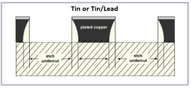
There are two different methods for inner and outer layer etching. In the outer layer etching process, tin plating is used as an etching resist. However, in the inner layer, the photoresist is a resist.
PCB wet etching method
Wet etching is an etching process in which unwanted materials are dissolved when immersed in a chemical solution.
PCB manufacturers jointly use two wet etching methods according to the etchant used.
Acid etching (ferric chloride and copper chloride).
Alkaline etching (ammonia)
These two methods have their pros and cons.
Acid etching process
The acid method is used to etch away the inner layer in the PCB board. This method involves chemical solvents such as iron chloride (FeCl3) or copper chloride (CuCl2). Compared with the alkaline method, the acidic method is more accurate, cheaper but time-consuming. This method is used for the inner layer because the acid does not react with the photoresist and does not damage the required part. In addition, the undercut in this method is minimal.
In order to project some light on the undercut, the undercut is the lateral erosion of the etching material under the protective layer. When the solution hits the copper, it attacks the copper and leaves tracks protected by electroplating etching resist or photoimaging resist. At the edge of the track, there is always some copper removed under the resist. This is called undercutting.

alkaline etching process
The alkaline method is used to etch the outer layer in the PCB board. Here, the chemical used is a combination of copper chloride (CuCl2Castle, 2H2O) + hydrochloride (HCl) + hydrogen peroxide (H2O2) + water (H2O). The alkaline method is a fast process and also a bit expensive. The parameters of this process must be strictly adhered to, because the solvent will damage the circuit board if it is exposed for a long time. This process must be well controlled.
The entire process is carried out in a conveyor-type high-pressure spray chamber, where the PCB is exposed to the renewed etchant spray. Important parameters to be considered during the PCB etching process are the speed at which the panel moves, the spray of chemicals and the amount of copper to be etched away. This ensures that the etching process evenly completes the straight side walls.
In the etching process, the etching point of the copper that is not needed is complete called the break point. This is usually achieved at the midpoint of the spray chamber. For example, if you consider the spray chamber length to be 2 meters, then when the circuit board reaches the midpoint, which is 1 meter, a breakpoint will be achieved.
The final product will have a circuit that meets the designer's specifications. Soon thereafter, the board of directors will proceed further for the divestiture. The stripping process removes electroplated tin or tin/lead or photoresist from the surface of the circuit board.
Therefore, this is an inside story about how the etching process occurs in the PCB board manufacturing unit. I hope this article can make you not feel the etching