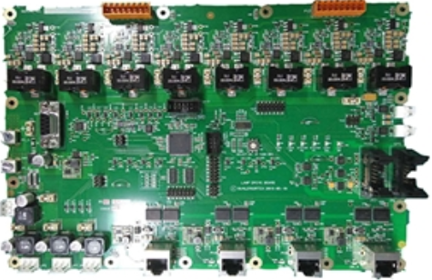
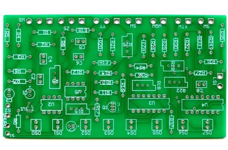
Talking about the line width and via hole of the circuit board
Circuit board manufacturer editor: We generally have a common sense when drawing circuit boards, that is, use thick wires (such as 50mil or even above) for large currents, and thin wires (such as 10mil) for small current signals.
For some electromechanical control systems, sometimes the instantaneous current flowing in the wire can reach more than 100A, so the thinner wire will definitely have a problem. A basic empirical value is: 10A/mm2, that is, the current value that a wire with a cross-sectional area of 1mm2 can pass safely is 10A. If the line width is too thin, the line will be burnt when a large current passes. Of course, the current burned traces also need to follow the energy formula: Q=I*I*t, for example, for a trace with 10A current, a 100A current burr suddenly appears and the duration is us level, then the 30mil wire is Definitely can bear it. (At this time, there will be another problem?? The stray inductance of the wire. This burr will generate a strong reverse electromotive force under the action of this inductance, which may damage other devices. The thinner the longer the wire is stray The greater the inductance, so the actual length of the wire must be considered)

The general circuit board drawing software often has several options when laying copper on the via pads of the device pins: right-angle spokes, 45-degree spokes, and straight laying. What is the difference between them? Novices often don't care much, just choose one at random and it's beautiful. actually not. There are two main considerations: one is to consider not cooling too fast, and the other is to consider the over-current capability.
The characteristic of the direct-laying method is that the overcurrent capability of the pad is very strong. This method must be used for the device pins on the high-power loop. At the same time, its thermal conductivity is also very strong. Although it is good for the heat dissipation of the device when it works, it is a problem for the circuit board soldering personnel. Because the heat dissipation of the pad is too fast and it is not easy to hang the tin, it is often necessary to use a larger wattage soldering iron and Higher welding temperature reduces production efficiency. The use of right-angle spokes and 45-angle spokes will reduce the contact area between the pins and the copper foil, and the heat dissipation is slow, and the soldering is much easier. Therefore, the choice of copper connection method for via-hole pads should be based on the application, and the overall overcurrent capability and heat dissipation capability should be considered together. Do not use direct routing for low-power signal lines, and for pads that pass large currents, they must be straight. shop. As for the right angle or the 45 degree angle, it looks good.
Why did you bring this up? Because I have been working on a motor driver for a while, the H-bridge components in this driver are always burned out, and I can't find the reason for four or five years. After my hard work, I finally found out: It turned out that the pad of a device in the power circuit was copper-plated with right-angle spokes (and because of the poor copper painting, only two spokes actually appeared) ). This greatly reduces the overcurrent capability of the entire power loop. Although the product has no problems during normal use, it is completely normal under the condition of 10A current. However, when the H bridge is short-circuited, a current of about 100A will appear on the loop, and the two spokes will be burnt instantaneously (uS level). Then, the power circuit becomes an open circuit, and the energy stored in the motor is emitted through all possible means without a discharge channel. This energy will burn the current-measuring resistor and related operational amplifier devices, and destroy the bridge control chip. And infiltrate into the signal and power supply of the digital circuit part, causing serious damage to the entire device. The whole process was as thrilling as a big landmine was detonated with a strand of hair. Then you may have to ask, why are only two spokes used on the pads in the power loop? Why not let the copper foil go straight? Because, hehe, the staff in the production department said that this pin is too difficult to solder! The designer just listened to the production staff, so... Hey, I found this problem really costing me a lot of brains, it's as simple as it sounds! Bitterness and happiness know oneself, bitterness and happiness know oneself...
If the via hole is less than 0.3mm, there is no way to use mechanical drilling. If laser drilling is used, the production and processing of the circuit board will be more difficult. So my personal opinion is that if it is not very necessary, the minimum is 0.5mm outside/0.3mm inside. . But like computer motherboards, memory modules, dense BGA packages, etc., sometimes it may be as small as 14mil/8mil. . My personal opinion is that the inner diameter of the hole is generally 1.5 times the line width. Of course, special thick lines (such as power supplies) do not need to be this way.