1 Overview
Almost every kind of electronic equipment, from watches and calculators on electronic wrists, to computers, communication electronic equipment, military weapon systems, as long as there are electronic components such as integrated circuits, must be used for electrical interconnection between them. Printed board. In the research process of larger electronic products, the most basic success factors are the design, documentation and manufacturing of the product's printed board. The design and manufacturing quality of printed boards directly affects the quality and cost of the entire product, and even leads to the success or failure of commercial competition.
1. The printed circuit provides the following functions in electronic equipment:
Provide mechanical support for fixing and assembling various electronic components such as integrated circuits.
Realize the wiring and electrical connection or electrical insulation between various electronic components such as integrated circuits.
Provide the required electrical characteristics, such as characteristic impedance.
Provide solder mask graphics for semi-automatic soldering, and provide distinguishable characters and graphics for component insertion, inspection, and maintenance.
2. Some basic terms related to PCB printed boards are as follows:
On the insulating base material, according to the predetermined design, the printed circuit, the printed element or the conductive pattern formed by the combination of the two are made, which is called the printed circuit.
On an insulating substrate, a conductive pattern that provides electrical connections between components and devices is called a printed circuit. It does not include printed components.
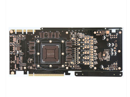
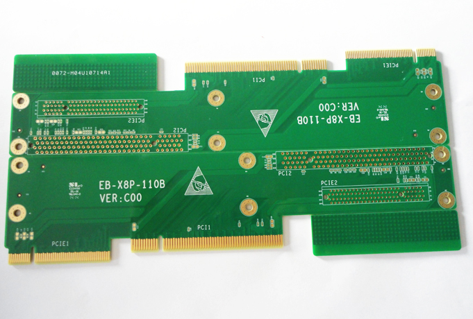
The printed circuit board still printed circuit is called the printed circuit board still printed circuit board, also known as the printed board.
Whether the substrate used for printed boards is rigid or flexible can be divided into two categories: rigid printed boards and flexible printed boards. Rigid-flexible combined printed boards have appeared this year. The number of layers following the conductor pattern can be divided into single-sided, double-sided and multilayer printed boards.
The printed board where the entire outer surface of the conductor pattern is on the same plane as the surface of the substrate is called a flat printed board.
For the terms and definitions of printed circuit boards, see the national standard GB/T2036-94 "Printed Circuit Terminology" for details.
After electronic equipment adopts printed boards, due to the consistency of similar printed boards, this avoids manual wiring errors, and can realize semi-semi-automatic insertion or placement of electronic components, semi-semi-automatic soldering, and semi-automatic detection, ensuring The quality of electronic equipment improves labor productivity, reduces costs, and facilitates maintenance.
Printed boards have developed from single-layer to double-sided, multi-layer and flexible, and still maintain their respective development trends. Due to the continuous development of high precision, high density and high reliability, continuous reduction of volume, cost reduction, and improvement of performance, printed boards will still maintain strong vitality in the development of electronic equipment in the future.

3. The sign of the technical level of the printed circuit board:
The technical level of the printed board is a sign of double-sided and multi-hole metallized printed boards: it is a double-sided metallized printed board produced in large quantities, two at the intersection of the 2.50 or 2.54mm standard grid Between the pads, the number of wires that can be laid as a sign.
A wire is laid between the two pads, which is a low-density printed board with a wire width greater than 0.3mm. Two wires are arranged between the two pads, which is a medium-density printed board with a wire width of about 0.2mm. Three wires are arranged between the two pads, which is a high-density printed board with a wire width of about 0.1-0.15mm. Arrange four wires between the two pads, which can be regarded as an ultra-high-density printed board with a line width of 0.05-0.08mm. "PCB circuit board" production process detailed explanation of the solar solder mask process The solar solder mask process in the printed circuit board is a printed board with solder mask after screen printing. Cover the pads on the printed board with a photo master so that it will not be irradiated by ultraviolet light during exposure, and the solder resist protection layer is more firmly attached to the printed board surface after ultraviolet light, and the pads are not exposed to ultraviolet light. Light irradiation can expose the copper pads so that lead and tin can be applied during hot air leveling.
(Detailed explanation of the solar soldering process in the PCB circuit board production process) The solar soldering process can be roughly divided into three operating procedures:
The first procedure is exposure. First, check whether the polyester film and glass frame of the exposure frame are clean before starting the exposure. If they are not clean, wipe them with an anti-static cloth as soon as possible. Then, turn on the power switch of the exposure machine, and then turn on the vacuum button to select the exposure program and shake it. Exposure shutter, before starting the formal exposure, you should let the exposure machine "empty exposure" five times. The function of "empty exposure" is to make the machine enter a saturated working state, and the most important thing is to make the UV exposure lamp + ray. Enter the normal range. If you don't "empty exposure", the energy of the exposure lamp may not enter the best working state. It will cause problems with the printed board during exposure. After five times of "empty exposure", the exposure machine has entered the best working condition. Before using the photographic plate for alignment, check whether the quality of the plate is qualified. Check whether there are pinholes and exposed parts on the film surface of the master plate, and whether it is consistent with the graphics of the printed board, because this will check the photo master to avoid rework or discard the printed board for unnecessary reasons.
Sun resist soldering generally adopts visual positioning, using a silver salt base plate, and align the pads of the base plate with the pad holes of the printed board, and fix them with tape to perform exposure. The solar resist soldering encountered in the alignment generally adopts visual positioning, using a silver salt master, align the pad of the master with the pad hole of the printed board, and fix it with tape for exposure. There are many problems encountered in alignment. For example, because the master plate is related to factors such
as temperature and humidity, if the temperature and humidity are not well controlled, the photographic master plate may be reduced or enlarged and deformed. In this way, the photo can be The bottom plate and the printed circuit board pads are not completely consistent. When the bottom plate is reduced, see how much the difference between the bottom plate pad and the printed board pad is. If the difference is small, lead-tin can be applied during hot air leveling, then there is no big problem for selenium resist soldering. If there is a big difference, only re-pirate, try to make the bottom pad overlap. Before aligning, you should also pay attention to whether the medicated film surface of the base plate is turned upside
down. Make sure that the medicated film surface is facing down during the alignment. The printed board does not need to be exposed to solder resist, which will cause the printed board to be scrapped. In addition, it should be noted that sometimes the imposition base plate does not overlap with the printed board graphics. Generally, the imposition base plate is cut along the edge of the imposition board, and then single-piece alignment is performed, and the entire printed board is aligned and exposed. The above problems are the ones that should be paid attention to before the formal exposure of selenium solder mask.
Then, perform solar resistance soldering, and check whether the printed board is sucked and covered by the vacuum box before exposure. The pressure of the vacuum suction cover should be sufficient and no dew gas exists. If the dew will cause the ultraviolet light to shine into the pattern along the side of the board, it will cause the shading part to be exposed,
and the development will not be off. Sometimes single-sided exposure is encountered. In this case, use a black cloth on the side without a pattern on one side. The ultraviolet light emitted by the exposure lamp is separated. If there is no black cloth, the ultraviolet light is transmitted into the pad through the side with no pattern so that the solder resist in the pad
hole cannot be developed after exposure. When exposing printed boards with different patterns on both sides, first screen-print one side of the solder mask, and then perform single-sided exposure. After development, screen-print the other side of the solder mask, because if both sides are screen-printed and exposed at the same time, one side has a complicated pattern. There are many pads, and there are many parts that need to be shaded, while the other side needs to be shaded less, so that ultraviolet light is transmitted
through one side to the other side, and the side with more shading is irradiated by ultraviolet light. Rework or discard. During the exposure process, it is also encountered that the printed board after the screen printing is not dried during curing. In this case, the special situation of the alignment makes the solder resist stick to the photo master. Moreover, the
printed board It also needs to be reworked, so if it is found that it does not dry, especially if most of the printed boards are not dried, they must be re-dried in the oven. These situations are problems that are prone to appear in the process of exposure, so we must carefully check, find out and solve them as soon as possible.
The second process is development. The developing operation is usually carried out in the developing machine, and the developing parameters such as the temperature of the developing solution, the delivery speed, and the spray pressure can be controlled to achieve a better developing effect. Development is to remove the solder mask on the pad with a developing solution to the shading part. The developing solution is one percent anhydrous sodium carbonate, and the liquid temperature is generally between 30 and 35 degrees Celsius. Before the formal development, the developer should be heated up to make the solution reach a predetermined temperature, because this achieves the best development effect.
The developing machine is divided into three parts:
The first section is the spray section, which mainly uses high-pressure spray of anhydrous sodium carbonate to dissolve the unexposed solder resist;
The second stage is the water washing stage. The first is to use high-pressure pump water to wash, first wash the remaining solution with water, and then enter the circulating water to wash, thoroughly wash;
The third section is the drying section. There is an air knife before and after the drying section, which mainly uses hot air to dry the board. If the temperature of the drying section is higher, the board can be dried.
The correct development time is clearly recognized by the display point. The display point must be maintained at a constant percentage of the total length of the development section. If the display point is too close to the exit of the development section, the unexposed solder mask will not be fully exposed. Development will cause the residue of the unexposed solder mask to remain on the board surface. If the display point is too close to the entrance of the development section, the exposed solder mask may be etched due to long-term contact with the developer. It becomes hairy and loses its luster.
The common display point is controlled within 40%-60% of the total length of the developing section. In addition, it should be noted that the board is easily scratched during the development. The common solution is to put the PCB board on the operator during the development. Gloves, the board should be handled gently, and the size of the printed board is different, so try to put the same size together. When placing the board, keep a certain distance between the board and the board to prevent transmission At times, the board is crowded, causing "jamming" and other phenomena. After showing the film, put the printed board on the wooden bracket.