On the insulating base material, according to the predetermined design, the printed circuit, the printed element or the conductive pattern formed by the combination of the two are made, which is called the printed circuit.

On an insulating substrate, a conductive pattern that provides electrical connections between components and devices is called a printed circuit. It does not include printed components.
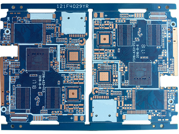
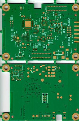
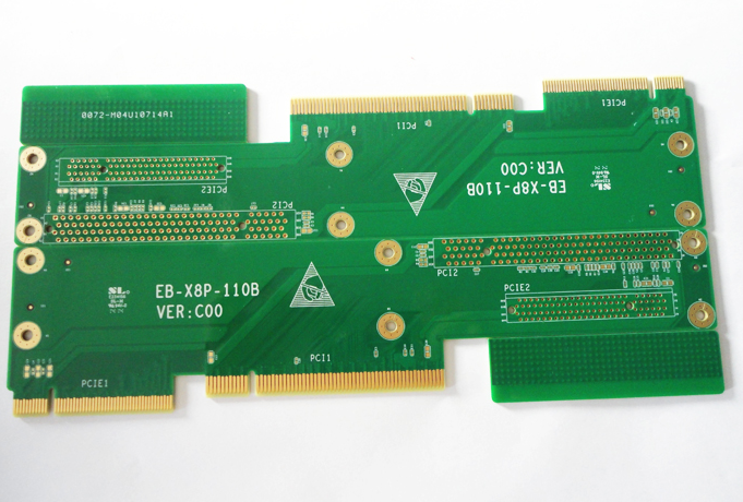
The printed circuit or the finished board of the printed circuit is called the printed circuit board or the printed circuit board, also known as the printed board.
Printed boards can be divided into two categories according to whether the substrate used is rigid or flexible: rigid printed boards and flexible printed boards. According to the number of layers of conductor patterns, it can be divided into single-sided, double-sided and multilayer printed boards.
The printed board where the entire outer surface of the conductor pattern is on the same plane as the surface of the substrate is called a flat printed board.
For the terms and definitions of printed circuit boards, see the national standard GB/T2036-94 "Printed Circuit Terminology" for details.
After electronic equipment adopts printed boards, due to the consistency of similar printed boards, manual wiring errors can be avoided, and electronic components can be automatically inserted or mounted, automatic soldering, and automatic detection, ensuring the quality of electronic equipment, Improve labor productivity, reduce costs, and facilitate maintenance.
Printed boards have developed from single-layer to double-sided, multi-layer and flexible, and still maintain their respective development trends. Due to the continuous development of high precision, high density and high reliability, continuous reduction of volume, cost reduction, and improvement of performance, printed boards will still maintain strong vitality in the development of electronic equipment in the future. three. The sign of the technical level of the printed board:
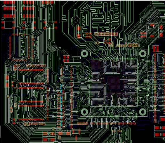
The technical level of the printed board is a sign of double-sided and multi-hole metallized printed boards: it is a double-sided metallized printed board produced in large quantities, two at the intersection of the 2.50 or 2.54mm standard grid Between the pads, the number of wires that can be laid as a sign.
A wire is laid between the two pads, which is a low-density printed board with a wire width greater than 0.3mm. Two wires are arranged between the two pads, which is a medium-density printed board with a wire width of about 0.2mm. Three wires are arranged between the two pads, which is a high-density printed board with a wire width of about 0.1-0.15mm. Arrange four wires between the two pads, which can be regarded as an ultra-high-density printed board with a line width of 0.05-0.08mm.