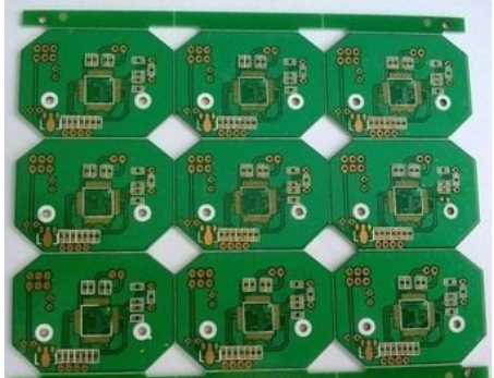
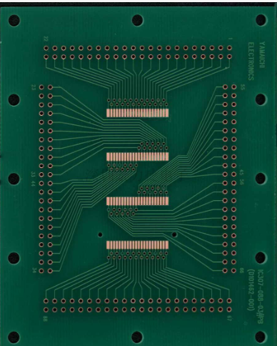
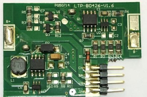
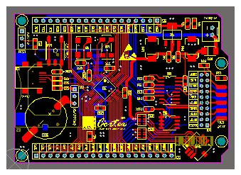
Printed circuit boards, also known as printed circuit boards, are providers of electrical connections for electronic components. Its development has a history of more than 100 years; its design is mainly layout design; the main advantage of using circuit boards is to greatly reduce wiring and assembly errors, and improve the level of automation and production labor rate. According to the number of circuit boards, it can be divided into single-sided boards, double-sided boards, four-layer boards, six-layer boards and other multilayer circuit boards.
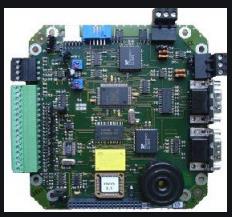
Since the printed circuit board is not a general terminal product, the definition of the name is a little confusing. For example, the motherboard used in personal computers is called the main board, and cannot be directly called the circuit board. Although there are circuit boards in the main board, They are not the same, so when evaluating the industry, the two are related but cannot be said to be the same. Another example: because there are integrated circuit parts mounted on the circuit board, the news media call it an IC board, but in fact it is not equivalent to a printed circuit board. We usually say that the printed circuit board refers to the bare board-that is, the circuit board without upper components.
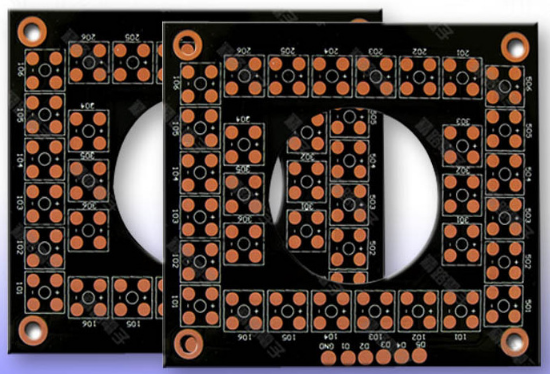
The following is an introduction to common problems and solutions for blanking printed circuit boards
★Causes of burrs:
1. The gap between the concave and the convex mold is too small, causing cracks on both sides of the convex mold and the concave mold without overlapping, and two extrusion shears occur at both ends of the section.

2. The gap between the concave and convex molds is too large. When the punch descends, the cracks will occur late, and the shearing will be completed like a tear, causing the cracks to not overlap.
3. The cutting edge is worn or rounded and chamfered, the cutting edge does not play a role in the division of the wedge, and the entire section produces irregular tears.
Solution:
1. Reasonably choose the blanking gap of the concave and convex dies. Such punching and cutting are between extrusion and stretching. When the punch cuts into the material, the cutting edge forms a wedge, causing the PCB board to produce nearly linear coincident cracks.
2. Refurbish the fillet or chamfer produced by the cutting edge of the concave and convex molds in time.
3. Ensure the vertical concentricity of the concave and convex molds to make the fit gap uniform.
4. Ensure that the mold installation is vertical and stable.
★Causes of bulging around the opening of the copper foil:
1. The blanking gap between the concave and convex dies is too small, and the punch edge becomes blunt. When the punch is inserted into the preheated and softened printed board, the plate will squeeze and move outwards and upwards around the punch.
2. The cutting edge of the punch has a taper. When the punch continues to enter the plate, the bulging around the orifice will increase as the taper of the punch increases.
Solution:
1. The blanking should exceed 20% of the original design thickness; otherwise, replace the plate or redesign the die.
2. The blanking should have enough pressing force to overcome the back-squeezing force of the material movement when punching;
★Turn up the copper port of the orifice
cause:
1. Due to the backlash, the copper foil is drawn into the punching gap of the concave and convex dies.
2. The bonding force between the copper foil and the substrate is poor. When the punch is pulled out of the printed board hole being punched, the copper foil is pulled up with the punch.
3. There is an inverted taper at the edge of the punch, which is swollen and deformed. When the punch is pulled out of the hole of the printed board, the copper foil will be pulled up with the punch.
Solution:
1. Use positive impact.
2. Replace the punch.
3. The clearance between the punch and the unloading plate should not be large, and a sliding fit should be used.
★ Causes of delamination and whitening around the face of the PCB substrate
1. The blanking gap between the concave and convex dies is inappropriate or the cutting edge of the concave mode becomes blunt. When punching, it is difficult for the punched sheet to form shear cracks at the edge of the concave pattern.
2. Substrate blanking performance is poor or not preheated before blanking.
3. The pressing force is small.
4. The leakage hole at the lower part of the die blade is blocked or the leakage resistance is large, resulting in swelling and stratification
Solution:
1. Reasonably expand the blanking gap between concave and convex dies;
2. Repair the blunt die cutting edge in time;
3. Increase the pressing force;
4. Adjust the preheating temperature of the substrate;
5. Enlarge or ream the leakage hole
★Inclination and deviation of the hole wall: the cause
1. The punch has poor rigidity, unstable centering, and tilts into the workpiece.
2. The installation of the punch is inclined or the clearance with the discharge plate is too large, and the discharge plate cannot provide precise guidance to the punch;
3. The matching clearance of the concave and convex molds is uneven. On the side with a small gap, the punch will receive a large radial force and slide to the side with a large gap;
4. The concentricity of the concave and convex mode assembly is poor; the pusher plate is out of position with the concave and convex molds; the matching accuracy of the pusher plate and the concave die is too poor (referring to compound blanking).
Solution:
1. Choose the material of the punch reasonably; improve the rigidity, strength, hardness and unevenness of the punch.
2. Improve the processing concentricity and assembly concentricity of the punch and the die.
3. Improve the matching accuracy of the punch and the discharge plate to ensure precise guidance.
4. Ensure the processing accuracy and assembly accuracy of the guide post and the guide sleeve; reduce the matching gap between the shape of the pusher plate and the die, and make the shape of the pusher plate consistent with the concave-convex shape.
★Causes of rough section
1. The blanking gap between the concave and convex dies is too large; the cutting edge of the concave die is severely worn.
2. The punching force of the punch is insufficient and unstable.
3. PCB board blanking performance is poor. For example, the base material contains too much glue, the base material, aging, and the lamination bonding force is low.
Solution
1. Choose the appropriate blanking gap between the concave and convex dies.
2. Trim the cutting edge of the die in time.
3Choose PCB substrates with better blanking performance and strictly control the preheating temperature and time according to the process requirements;
★Causes of the cracks between the holes and the holes
1. The hole wall is too thin, and the radial pressing force during punching exceeds the strength of the hole wall of the printed board substrate.
2. The two adjacent holes are not punched out at the same time. When the punch enters the plate, the hole wall is too thin and cracked.
Solution
1. The design of the hole spacing on the PCB printed board should be reasonable, and the hole wall should not be less than the thickness of the substrate.
2. The adjacent holes should be punched out at the same time with a pair of molds.
3. Make two punches that are very close to each other into different lengths with a difference of 0.5mm, so that the more concentrated punching force in a small area can be dispersed instantaneously.