How to improve the damage and penetration of dry film in PCB production
iPCB has summarized part of the production experience in the circuit board production process for many years, especially for the production of some multi-layer PCB circuit board, especially for those boards with line width and line spacing of 3mil and 3.5mil. For circuit etching, The requirements for graphics transfer are very high, not only for equipment, but also for manual experience. The so-called "slow work produces meticulous work", high-quality goods take time to forge!
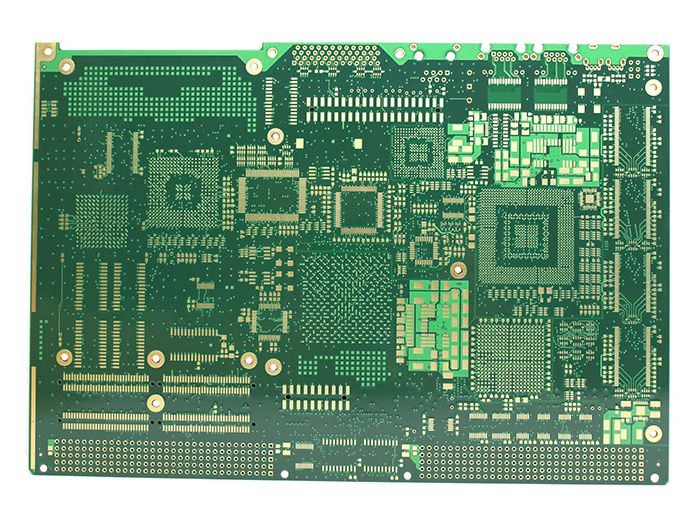
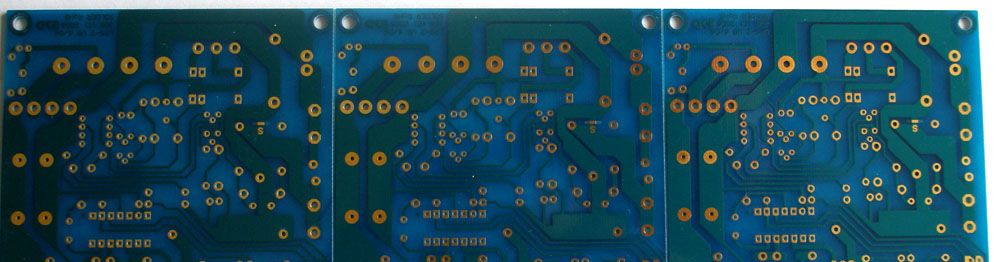
For PCB multi-layer circuit boards, its wiring is very precise, and many circuit board manufacturers use dry film technology to transfer circuit patterns, but in the production process, many PCB manufacturers have many misunderstandings when using dry film.
One, the dry film produced by the circuit board has holes when the holes are masked
Many customers mistakenly believe that after a hole occurs, the film temperature and pressure should be increased to enhance its bonding force. However, this idea is incorrect. After the temperature and pressure become higher, the corrosion resistance Excessive volatilization of the solvent of the layer makes the dry film more brittle and thinner. It is easy to be broken during development. The toughness of the dry film must be maintained during production. Therefore, after the production of broken holes, the circuit board manufacturer recommends that you start from the following Make improvements in several areas:

1. Reduce the temperature and pressure of the film;
2. Improve the hole wall roughness and drape;
3. Reduce the pressure of developing;
4. Increase the energy of exposure;
5. When applying the film, the dry film we use should not be stretched too tightly;
6. Do not park for too long after applying the film, so as not to cause the semi-fluid film to diffuse and thin at the corners.
Two, seepage plating occurs during dry film plating in the production of circuit boards
The occurrence of seepage indicates that the dry film and the copper foil are not firmly adhered, so that the electroplating solution enters, and then the "negative phase" part of the plating layer becomes thicker. Most circuit board manufacturers have seepage plating, which is caused by the following bad reasons :
The film temperature is too high or low
If the film temperature is too low, the resist film cannot be sufficiently softened and flowed properly, resulting in poor adhesion between the dry film and the surface of the copper clad laminate; if the temperature is too high, the solvent and other volatility in the resist The rapid volatilization of the substance produces bubbles, and the dry film becomes brittle, causing warping and peeling during electroplating electric shock, resulting in infiltration.
1. The film pressure is too high or low
When the film pressure is too low, it may cause uneven film surface or gaps between the dry film and the copper plate and fail to meet the requirements of the bonding force; if the film pressure is too high, the solvent and volatile components of the resist layer will volatilize too much, causing The dry film becomes brittle and will be lifted and peeled after electroplating electric shock.
2. The film temperature is too high or low
If the film temperature is too low, the resist film cannot be sufficiently softened and flowed properly, resulting in poor adhesion between the dry film and the surface of the copper clad laminate; if the temperature is too high, the solvent and other volatility in the resist The rapid volatilization of the substance produces bubbles, and the dry film becomes brittle, causing warping and peeling during electroplating electric shock, resulting in infiltration.
3. Exposure energy is too high or low
Under ultraviolet light irradiation, the photoinitiator, which has absorbed the light energy, decomposes into free radicals to initiate a photopolymerization reaction to form a body-shaped molecule that is insoluble in a dilute alkali solution. When the exposure is insufficient, due to incomplete polymerization, the film swells and becomes soft during the development process, resulting in unclear lines or even the film layer falling off, resulting in poor bonding between the film and copper; if the exposure is overexposed, it will cause development difficulties and also during the electroplating process. Warping and peeling occurred during the process, forming penetration plating. Therefore, it is very important to control the exposure energy.