In hardware system design, the crosstalk that we usually pay attention to mainly occurs between connectors, chip packages, and parallel traces with relatively close spacing. However, in some circuit board designs of PCB factories, large crosstalk between high-speed differential vias will also occur. The editor of the PCB factory provides example simulation analysis and solutions for the crosstalk between high-speed differential vias.
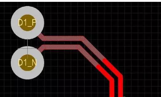
Crosstalk between high-speed differential vias
For thicker PCBs, the thickness may reach 2.4mm or 3mm. Take a 3mm single board as an example. At this time, the length of a through hole in the Z direction on the PCB can reach nearly 118 mils. If there is a 0.8mm pitch BGA on the PCB, the fan-out via pitch of the BGA device is only about 31.5mil.
As shown in Figure 1, the parallel length H in the Z direction between two pairs of adjacent differential vias is greater than 100 mils, and the horizontal distance between the two pairs of differential vias is S=31.5 mil. When the parallel distance between vias in the Z direction is much larger than the horizontal distance, the crosstalk problem between high-speed signal differential vias must be considered. By the way, when designing high-speed PCBs, the length of the via stub should be minimized as much as possible to reduce the impact on the signal. As shown in Figure 1 below, the stub will be shorter if it is routed close to the Bottom layer. Or you can use back drilling.
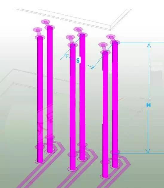
Figure 1: Crosstalk generated by high-speed differential vias (H>100mil, S=31.5mil)
Simulation Analysis of Crosstalk Between Differential Vias
The following is a simulation of a design example with a board thickness of 3mm, a 0.8mm BGA fan-out via pitch of 31.5mil, and a via parallel distance H=112mil.
As shown in Figure 2, we define 4 pairs of differential pairs into 8 differential ports according to the routing.
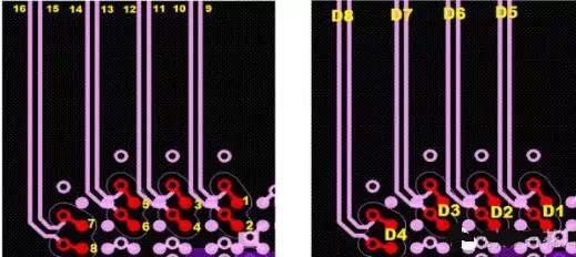
Figure 2: Crosstalk simulation port definition
Assuming that the differential ports D1-D4 are the receiving ends of the chip, we analyze the crosstalk of adjacent channels by observing the far-end crosstalk of the D5, D7, and D8 ports to the D2 port. From the results shown in Figure 3, we can see that the far-end crosstalk between the two channels at a relatively close distance can reach -37dB@5GHz and -32dB@10GHz, and further optimization of the design is needed to reduce the crosstalk.
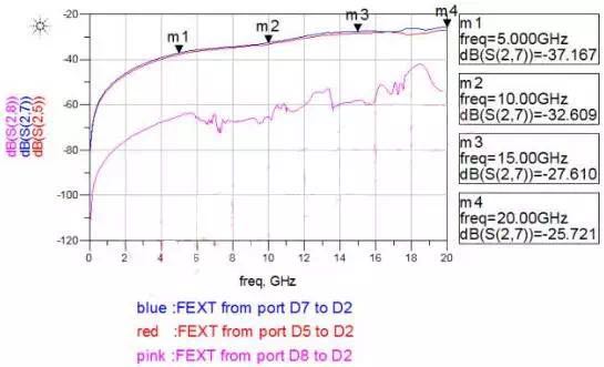
Figure 3: Crosstalk simulation results between differential pairs
You may have questions after reading this: How to determine the crosstalk caused by the differential vias rather than the crosstalk caused by the differential traces?
In order to illustrate this problem, we divide the above-mentioned example into two parts, BGA fan-out area and differential traces, for simulation respectively. The simulation result is shown in Figure 4:
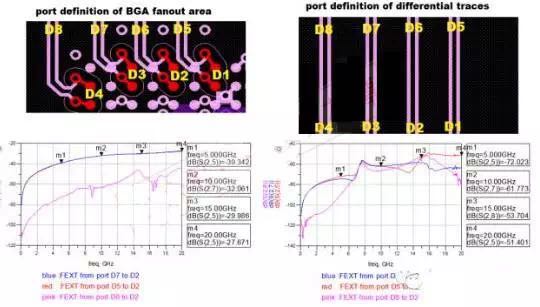
Figure 4: BGA fan-out area and differential trace crosstalk simulation results
From the simulation results on the right side of Figure 4, it can be seen that the crosstalk between the differential traces is below -50dB, and even reaches below -60dB in the 10GHz frequency band. The crosstalk in the fan-out area of the BGA is relatively close to the crosstalk value of the original overall simulation. From the simulation results in Figure 4, we can conclude that the crosstalk between the differential vias in the above example plays a major role.
Optimization of crosstalk between differential vias
Knowing the root causes of crosstalk caused by such problems, the method of optimizing crosstalk between differential vias is clearer. Increasing the spacing between differential vias is a simple, easy and effective method. Based on the original design of the example, we optimized the position of the differential vias so that the spacing between each pair of differential vias is greater than 75 mils. From the simulation results shown in Figure 5 and the data comparison in Table 1, it can be seen that the optimized far-end crosstalk has an improvement of 15-20dB in the 15GHz band and 10dB in the 15-20GHz band compared to the original design.
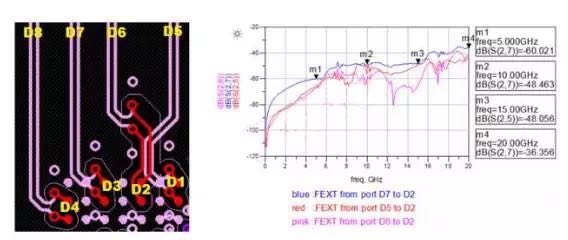
Figure 5: Crosstalk simulation results after optimizing the spacing of differential vias
