According to the specific characteristics of the PCB factory circuit board, choose the method of online testing to combine one or more processes, learn from each other's strengths, and use them comprehensively. Now let's introduce the method of intelligent detection of PCB factory circuit boards.
First of all, adopt the idea of virtual instrument on the PCB board machine to establish related application software, that is, realize various functions of traditional instruments through software, including oscilloscope, signal generator, and various mathematical processing of collected data. During the test, a digital signal is given through the test software.
Then, the PCB board test system will have a new design idea. The design idea of the automatic test system and virtual instrument based on the USB bus will be adopted to give full play to the role of the computer. The idea of replacing the traditional instrument with a computer is minimized. The volume of the instrument itself is reduced, the development cost is reduced, and the development efficiency is improved.
Next, after D/A conversion, the analog excitation signal required for the test is applied to the test system, and then sent from the test circuit to the switch matrix through the test bus. The switch matrix is connected to the switch matrix while being controlled by the microprocessor. When the circuit breaks, the tested PCB board is fixed on the needle bed, the excitation signal is applied to the corresponding position of the printed circuit board, and the response is measured by the test circuit, and the collected analog quantity is sent to the core control, after A/D conversion, Get the corresponding digital quantity, feedback from the software on the PCB machine and process the PCB machine to determine whether the PCB board is qualified.

This online testing technology breaks through the previous method of using human eyes to detect circuit boards. The online testing technology has high efficiency and low missed detection rate, and realizes the automation of the detection field. This detection system adopts the idea of combining with virtual instruments, which reduces the design of hardware and reduces the cost of the entire system.
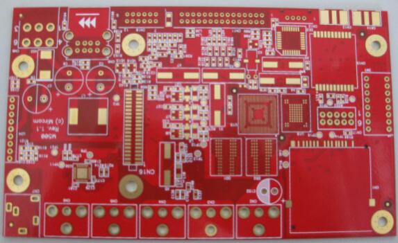
PCB circuit boards have developed from single-layer to double-sided, multi-layer and flexible, and still maintain their respective development trends. Due to the continuous development of high precision, high density and high reliability, continuous reduction in size, cost reduction, and performance improvement, PCB circuit boards still maintain a strong vitality in the development of electronic equipment in the future. The following editor will introduce which parts of the circuit board need to be processed.
1. Circuit and pattern (Pattern): The circuit is used as a tool for the conduction between the originals. In the design, a large copper surface will be additionally designed as a grounding and power layer. The route and the drawing are made at the same time.
2. Dielectric layer (Dielectric): Used to maintain the insulation between the circuit and each layer, commonly known as the substrate.
3. Hole (Through hole / via): The through hole can make the lines of more than two levels connect to each other. The larger through hole is used as a part plug-in. In addition, there are non-through holes (nPTH) usually used as Surface mount positioning, for fixing screws during assembly.
4. Solder resistant /Solder Mask: Not all copper surfaces need to be tinned parts, so the non-tin area will be printed with a layer of material that isolates the copper surface from eating tin (usually epoxy resin), To avoid short circuits between non-tinned circuits. According to different processes, it is divided into green oil, red oil and blue oil.
5. Silk screen (Legend/Marking/Silk screen): This is a non-essential structure. The main function is to mark the name and position frame of each part on the circuit board, which is convenient for maintenance and identification after assembly.
6. The surface finish of the PCB manufacturer: Because the copper surface is easily oxidized in the general environment, it can not be tinned (poor solderability), so it will be protected on the copper surface that needs to be tinned. The protection methods include HASL, ENIG, Immersion Silver, Immersion Tin, and Organic Solder Preservative (OSP). Each method has its advantages and disadvantages, which are collectively referred to as surface treatment.