Detailed explanation of PCB circuit board gold finger production
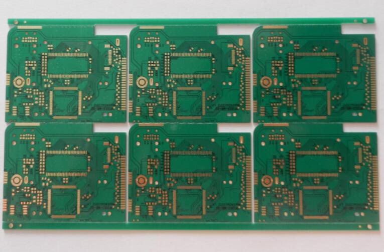
The gold finger PCB is composed of many golden yellow conductive contacts. Because its surface is gold-plated and the conductive contacts are arranged like fingers, it is called "golden finger". The gold finger is actually a layer of gold on the copper clad board through a special process, because gold has strong oxidation resistance and strong conductivity, but it is expensive. Many motherboards, memory and graphics cards are the "gold finger "Use brass material instead of gold.
All the data flow and electronic flow of the memory processing unit are exchanged with the PC system through the contact of the golden finger and the memory slot, which is the output and input port of the memory, so the manufacturing process is very important for the memory connection.
PCB circuit board gold finger production
1. Surface treatment method of gold finger
1.Gold-plated
Gold plating, also known as "electroplating gold", "electroplating nickel gold", "electrolytic gold", etc., refers to the method of electroplating to make gold particles adhere to the PCB board. Because of the strong adhesion, it is also called "hard gold". Gold plating can greatly increase the hardness and wear resistance of PCB, can effectively prevent the diffusion of copper and other metals, and can meet the requirements of hot-press welding and brazing; the plating layer is uniform and detailed, low porosity, low stress, and good ductility .

2. Immersion gold
Immersion gold, also known as "nickel immersion gold", "nickel gold", "nickel gold", "metal gold", is a chemical reaction to make gold particles adhere to the PCB pads because of weak adhesion, Also known as "soft gold". Immersion gold can enable PCB to achieve good electrical conductivity during long-term use, and it also has environmental tolerance that other surface treatment processes do not have.
3. The difference between Immersion Gold and Gold Plated:
(1) The crystal structure formed by the two is different. Immersion gold is much thicker than gold plating. Immersion gold is golden yellow, which is more yellow than gold plating (this is one of the ways to distinguish between gold plating and immersion gold) .
(2) Immersion gold is easier to weld than gold plating and will not cause poor welding.
(3) There is only nickel and gold on the pads of the immersion gold board, and the skin effect of the signal is transmitted on the copper layer, which will not affect the signal.
(4) Immersion gold is denser than gold-plated crystal structure, and it is not easy to produce oxidation.
(5) Gold plating is easy to short-circuit the gold wire. However, there is only nickel and gold on the pads of the immersion gold board, and there is no short circuit of the gold wire.
(6) There is only nickel and gold on the pads of the immersion gold board, so the bonding of the wire resistance and the copper layer is stronger.
(7) Immersion gold plate has better flatness and service life than gold plate.
2. Gold finger cut copper production
1. The width of copper cut in the inner layer of the gold finger area = the depth of the lead angle + 0.25MM.
2. Cut the copper from the outer gold finger to the edge of the board:
(1) When the customer requires that the gold finger is not allowed to expose the copper, CAM cuts the copper according to the chamfer depth +0.15MM;
(2) When the customer allows the finger to expose the copper, cut the copper to 50% of the plate thickness.
3. When the distance between the golden finger area and the non-gold finger area is less than 7mm, the inner conductor of the non-gold finger area should be cut according to the corresponding requirements of the inner chamfer depth to cut the copper to prevent the copper from being exposed during the chamfering.
4. If the customer's outer gold finger is far from the edge of the board, there is no need to cut copper internally; if the inner layer needs to cut copper, it is 0.15mm more unilateral than the outer gold finger.
1. The gold finger spacing designed by the customer's manuscript is ≥6mil. If the gold finger spacing is less than 6mil, it is recommended that the customer make the gold finger thinner.
2. Add a fake finger to disperse the current on both sides of the board outside the gold finger area, and add gold fingers for each group. At least two fake fingers should be added to the gong empty position or the edge of the panel.
3. Lead design, the width of the main lead is 20mil.
Four, gold finger solder mask production
1. All PTH holes with a distance of ≤1mm from the golden finger must be covered with oil (the hole can be plugged when the hole diameter is ≤0.5mm).
2. For the gold finger solder mask, the entire window must be opened, and the window must be opened to the edge of the board, but the distance between the solder mask and the adjacent conductor in the gold finger area must be 1mm.
3. The fake finger must be soldered to open the window.
4. If the customer's manuscript gold finger has a design solder mask bridge position, the EQ will open the window for the customer.
Five, gold finger shape (chamfering)
The golden finger needs to be chamfered, usually 45°, other angles such as 20°, 30°, etc. If there is no chamfer in the design, there is a problem. iPCB is a high-tech manufacturing enterprise focusing on the development and production of high-precision PCBs. iPCB is happy to be your business partner. Our business goal is to become the most professional prototyping PCB manufacturer in the world. Mainly focus on microwave high frequency PCB, high frequency mixed pressure, ultra-high multi-layer IC testing, from 1+ to 6+ HDI, Anylayer HDI, IC Substrate, IC test board, rigid flexible PCB, ordinary multi-layer FR4 PCB, etc. Products are widely used in industry 4.0, communications, industrial control, digital, power, computers, automobiles, medical, aerospace, instrumentation, Internet of Things and other fields.