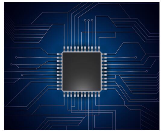
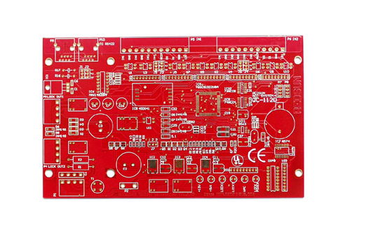
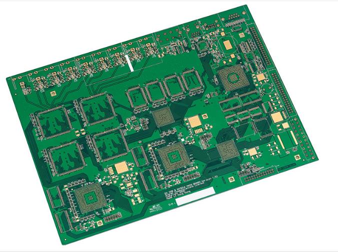
PCB manufacturer: What are the processes for the copper sinking process?
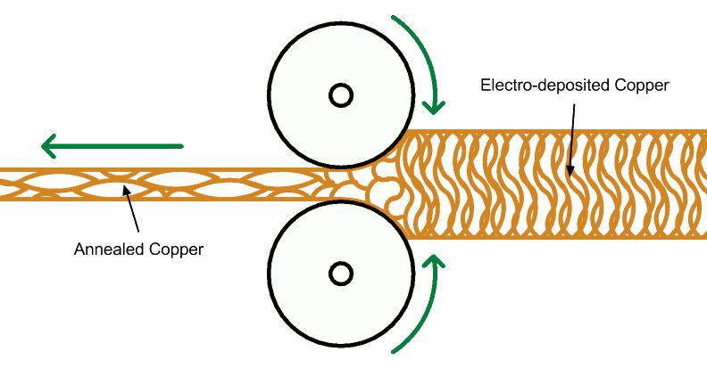
PCB manufacturer: Immersion copper is the abbreviation of electroless copper plating, also called plated through hole, abbreviated as PTH, which means that a thin layer of chemical copper is deposited on the non-conductive hole wall substrate that has been drilled., As a base for electroplating copper later.
PTH process: alkaline degreasing-two or three-stage countercurrent rinsing-coarsening (micro-etching)-secondary countercurrent rinsing-pre-soaking-activation-secondary countercurrent rinsing-degumming-secondary countercurrent rinsing-copper deposition-secondary Countercurrent rinsing - pickling.
Detailed explanation of the process:
1. Alkaline degreasing: remove oil stains, fingerprints, oxides, and dust on the surface of the board; adjust the wall of the hole from negative charge to positive charge, which facilitates the adsorption of colloidal palladium in the subsequent process.
2. Micro-etching: remove oxides on the board surface, roughen the board surface, ensure that the subsequent copper immersion layer has a good bonding force with the bottom copper of the substrate, and can well adsorb colloidal palladium;
3. Pre-soaking: It is mainly to protect the palladium tank from the contamination of the pre-treatment tank solution, prolong the service life of the palladium tank, and effectively wet the hole wall, so that the subsequent activation solution can enter the hole in time for sufficient and effective activation;
4. Activation: After the polarity of the alkaline degreasing is adjusted by the pretreatment, the positively charged pore wall can effectively adsorb enough negatively charged colloidal palladium particles to ensure the average, continuity and compactness of the subsequent copper precipitation.

5. Degumming: remove the stannous ions from the colloidal palladium particles to expose the palladium nucleus in the colloidal particles to directly and effectively catalyze the chemical copper deposition reaction.
6. Copper sinking: The electroless copper sinking autocatalytic reaction is induced by the activation of the palladium nucleus. Both the new chemical copper and the reaction by-product hydrogen can be used as reaction catalysts to catalyze the reaction, so that the copper sinking reaction continues. After processing through this step, a layer of chemical copper can be deposited on the board surface or the hole wall.
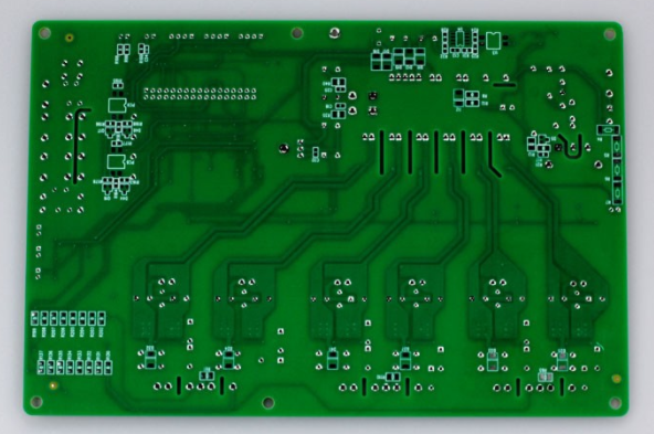
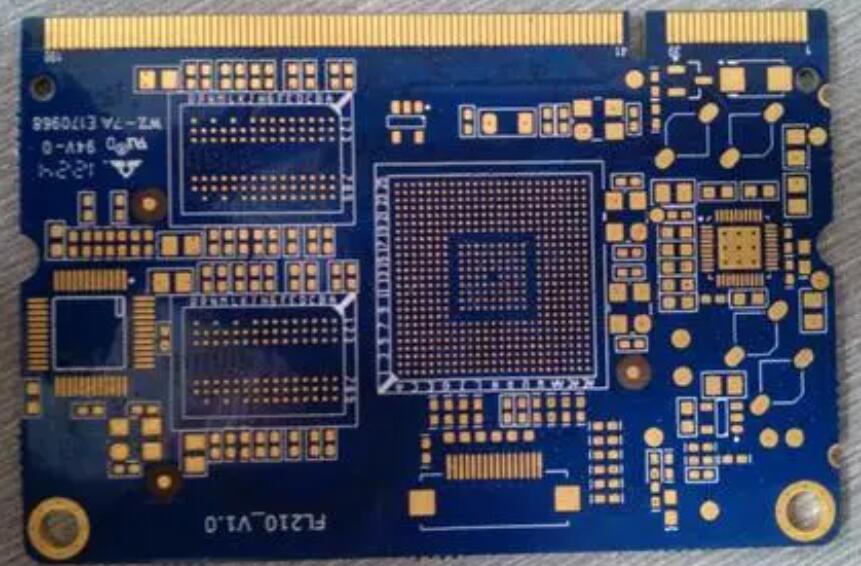
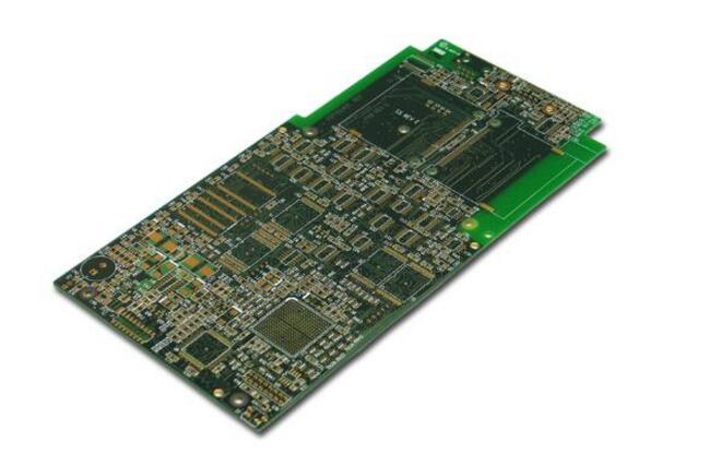
The quality of the copper sinking process is directly related to the quality of the production circuit board. It is the main source process of impermissible vias and poor open and short circuits. It is inconvenient for visual inspection. The subsequent processes can only be screened probabilistically through destructive experiments. For effective analysis and monitoring of a single PCB board, it is necessary to strictly follow the parameters of the work instruction. It can be seen that it is particularly important to find a suitable PCB proofing manufacturer. ipcb is a high-precision, high-quality PCB manufacturer, such as:isola 370hr PCB, high-frequency PCB, high-speed PCB, ic substrate, ic test board, impedance PCB, HDI PCB, Rigid-Flex PCB, buried blind PCB, advanced PCB, microwave PCB, telfon PCB and other ipcb are good at PCB manufacturing.