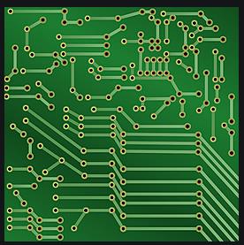
After the entire circuit board design is completed, the PCB circuit boardneeds to be SMT patched and attached to the components. Each SMT processing factory will specify the most suitable size of the circuit board according to the processing requirements of the assembly line, for example, the size is too large. If it is too small or too large, the tooling for fixing the circuit board on the assembly line cannot be fixed. So the question is, what if the size of our circuit board itself is smaller than the size specified by the factory? That is, we need to put the circuit boards together, and put multiple circuit boards into one piece. Imposition can significantly improve efficiency for both high-speed placement machines and wave soldering.
When making imposition, you can easily separate multiple boards to avoid damage to the circuit board during the separation. Determine which type of board to use according to the shape of a single type of your imposition. PCB imposition methods mainly include V-CUT, punching, and stamp hole. The size of the panel can not be too large or too small. Generally, small boards can be assembled or welded for convenience.
1. PCB assembly method-V-CUT
V-CUT means that several boards or the same board can be combined and spliced together, and then after the PCB processing is completed, a V-cut machine is used to cut a V-shaped groove between the boards, which can be broken during use. It is the more popular way nowadays.
2. PCB assembly method-punching groove
Punching refers to milling out between the board or the inside of the board with a milling machine as needed, which is equivalent to digging out.
3. PCB jigsaw method-stamp hole

The so-called stamp use is to use a small hole to link the board to the board, which looks like the zigzag on the stamp, so it is called the stamp hole link. The stamp hole link requires high-control burrs on all four sides between the board and the board, that is, only a small stamp hole can be used to replace the V line.
iPCB is happy to be your business partner. Our business goal is to become the most professional prototyping PCB manufacturer in the world. With more than ten years of experience in this field, we are committed to meeting the needs of customers from different industries in terms of quality, delivery, cost-effectiveness and any other demanding requirements. As one of the most experienced PCB manufacturers and SMT assemblers in China, we are proud to be your best business partner and good friend in all aspects of your PCB needs. We strive to make your research and development work easy and worry-free.
quality assurance
iPCB has passed ISO9001:2008, ISO14001, UL, CQC and other quality management system certifications, and produces standardized and qualified PCB products. We master complex process skills and use professional equipment such as AOI and Flying Probe to control production, X-ray inspection machines, etc. . Finally, we will use double FQC inspection of appearance to ensure shipment under IPC II standard or IPC III standard.
Our factory is located in China. For decades, Shenzhen has been known as the world's electronics R&D and manufacturing center. Our factory and website are approved by the Chinese government, so you can skip the middlemen and buy products on our website with confidence. Because we are a direct factory, this is the reason why 100% of our old customers continue to purchase on iPCB.