PTFE circuit board processing technology introduction
Microwave high multilayer circuit board technology
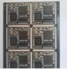
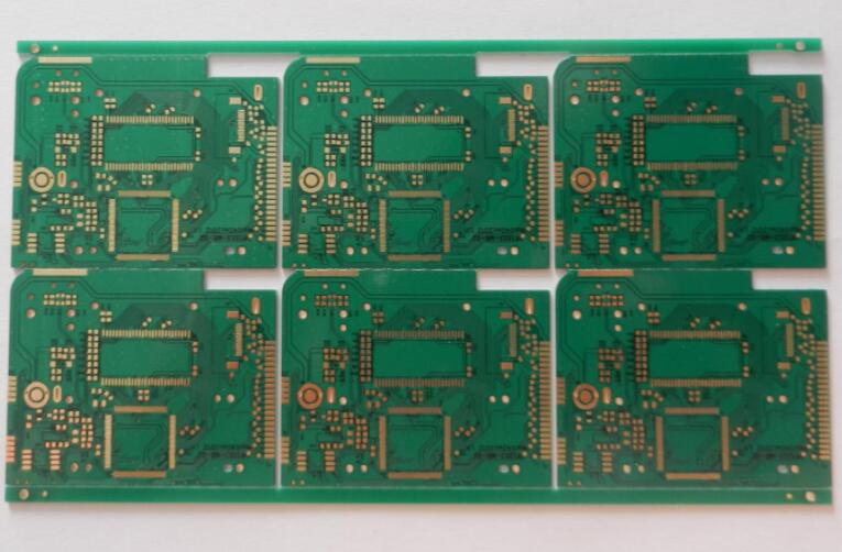
With the increasing frequency in the microwave field, PTFE multilayer board is used as a microwave device and high-speed back PTFE multilayer board technology to carry out a 12-layer PTFE multilayer board model.
Experimental design 1 The sample board requires DK=3.0, Df=0.0023 (10G Hz), thickness 3.7mm, step groove structure, and two-layer alignment +/-0.01mm.
1.1 Substrate selection
1.1.1 Classification of plates The plates can be divided into 5 categories:
1. PTFE+glass cloth. Poor workability.
2. PTFE+non-woven glass cloth. Good workability.
3. PTFE+ceramic packing has the best workability.
4. PTFE+glass cloth+ceramic packing. Performance is slightly better than pure PTFE plus glass cloth processability.
5. PTFE adhesive sheet is divided into: PTFE adhesive sheet, BT wrapped PTFE prepreg, PTFE semi-solid. According to the performance requirements of the model and the material performance and price, we make the following material selection: The core plate is the most difficult to process PTFE + glass cloth and PTFE+glass cloth+ceramic filler material PTFE bonding sheet.
1.1.2 Sheet characteristics
a. Physical and chemical properties PTFE material has excellent electrical properties and good chemical stability. Its dielectric constant is low, and between, the change with frequency is not obvious, the dielectric constant of 1G and 10G basically does not change, so it is commonly used here that we mainly apply this kind of performance. After adding ceramic filler

b. Processing characteristics PTFE sheet has very poor processing properties. The material is soft, and there is little PTFE flow glue when pressed. The PTFE material itself has the following problems: When the sheet is made, the bonding force between the filler and glass fiber impregnated by the glass fiber is small, and the amount of glue flow is small, and there is no mutual Bonding force, so it is easy to drill the glass
1. The TFE material itself has a low polarity, and the bonding force between the substrate and the copper foil between the substrate and the glass cloth is poor, and the printed solder mask is also difficult, and the plate is not resistant to mechanical impact. PTFE and glass
2. The material is soft, the material is soft, easy to deform, the support for glass fiber and copper foil is small, plus the problem 1. It is easy to deform by mechanical force and the cutting effect of glass fiber is not good when drilling, and it is not easy to cut at one time, and PTFE is also easy Produce uncut PTFE drill chips.
c. Brief introduction of PTFE bonding sheet PTFE bonding sheet: a transparent thermoplastic bonding sheet, the thickness is generally 1.5mil,3.0mil. Dielectric 2.3, the dielectric loss is that the pressing temperature is above 220 degree Celsius, there is less glue flow, and it is easy to have non-flowing glue.
1.1.3 Results of material selection According to sample requirements and test requirements, we select materials from suppliers A, B, and C for testing, with core DK=2.5~3.5.
The sample material is DK=3.0(10GHz), Df=0.0023(10Ghz).
2 factor analysis
From the characteristics of the material, we know that the main problems in the processing of PTFE multi-layer boards are concentrated in pressing, drilling, and ink printing.
In view of the above problems, we make the following experimental method design.
3 Process method design
3.1 Drilling holes. Because the material is relatively soft and the glass fiber is relatively soft, it is easy to produce burrs. Therefore, it is necessary to add a relatively hard special PTFE material. Small drilling speed (need to be determined by experiment.
Since there is no resin bonding between the glass fibers, there is no drill hole between each other without cutting. It is easy to produce uncut glass fibers, and electroplating forms plating nodules.
At the same time, the PTFE material is relatively soft, and the PTFE material may remain on the hole wall without being cut.
Because the resin on the cover plate and the backing plate will stick to the hole wall under high temperature, it will also part of the drill cuttings (PTFE. Because the packing of each PTFE material, the choice of glass cloth, etc., are different, it may be different for each material. In view of the above analysis, we will mainly focus on the selection of pad cover, drilling parameter test, bit type
a. Choosing the pad cover It is currently ideal to use phenolic resin material for the pad cover. This kind of board material is relatively hard, but the phenolic resin
b. Parameter test
1. Test method It is the first time for the tester to test the drilling parameters of the material, and the drilling characteristics of the material cannot be understood more accurately. The drilling parameters of PTFE are used as the benchmark, according to the single-drilling feed amount (comprehensive parameters of speed and feed amount). And based on experience and theoretical analysis, some parameter combinations that can be used with a small probability are removed.
On this basis, perform a larger range of parameter combinations in this direction. After the test is completed, perform parameter combinations in this small range to determine the more accurate parameters. 2. Tool selection tool We choose the following diameter as the test tool: Ф0. 5mm, Ф1.0mm, Ф1.5mm, Ф2.0mm, Ф3.0mm, Ф3.2mm, Ф4.5mm.
4. Test method After drilling the hole, wash it twice with high-pressure water, observe the inside of the hole with a magnifying glass under 25 times strong light, and judge the inside of the hole with a 25 times magnifying glass. Finally, make a section to observe the drilling situation and determine the maximum number of holes used by the drill by investigating the situation of the wound drill bit and the wear of the drill bit. For the final 5 times of impact test, confirm its reliability.
3.2 Porosity-electroplating Because PTFE material has a small polarity and is not easy to combine with other materials, it is difficult to sink copper, and it is necessary to find a way. At the same time, because the drilling will definitely leave uncut fibers and resin and resin sticking to the hole wall Regarding the difference between PTFE material and FR-4, we mainly focus on de-drilling (removing hole wall drilling and its sticking) and ensuring the reliability of copper sinking.
Since it is difficult to sink copper for PTFE materials, the current three-time copper-immersion and three-time electroplating method is used for copper-immersion electric multilayer boards. PLASMA is required for de-drilling and activation treatment to ensure the reliability of PTH.
Due to the softness of PTFE material, during electroplating, the swing in the electroplating tank will easily break the plate or make the plate reliable.
3.3 Solder mask-leveling (golding) PTFE material itself has very little binding force with ink. Because PTFE material core board is pressed together, PTFE and ink are applied to the surface to prevent the surface activation layer from failing, resulting in poor adhesion between the ink and the board. good.
Another process method is needed to activate the surface of the etched PTFE material with PLASMA. The factors that affect the ink binding force include mechanical damage, such as brushing, scratching, impact, etc., so the solder mask is due to the pores of the PTFE material. The wall condition is not very good, and the first copper plating of the hole wall will leave the hole wall liquid vaporizing too fast, leading to blistering and other phenomena at the orifice.
Preliminary determination is to use step-by-step upgrades for post-curing parameters to be evaluated. In the same way, we determine the parameters of the baking sheet after chemical nickel-gold through experiments on the parameters of the baking sheet before leveling.
After the gold is melted, the baking time is too long, the solderability is not enough, and the reflow soldering may cause delamination and blistering, so the baking parameters need to be evaluated.
3.3.1 Evaluate the time interval from etching to ink printing. After etching, wait 6 hours, 8 hours, 12 hours, 16 hours, 24 hours, and 36 hours to start 3M tape and test the ink structure.
3.3.2 Determine the post-curing parameters of the ink Test the post-curing parameters of the ink.
3.3 PTFE multi-layer board After the above problems are solved, the difficulty of multi-layer board mainly focuses on process control, lamination, drilling, and copper immersion-the multi-layer board has basically completed the compression parameter test at present, and the drilling problem is relatively large. Without PLASMA,
3.3.1 Pressing parameters a. Pressing conditions Since the pressing temperature of the PTFE adhesive sheet is high, we were worried about the press problem at first. The maximum pressing temperature is 220 degree Celsius, and the pressure parameters provided by the supplier are also relatively small (700~1400Kpa) ).
According to the above parameters, the peel strength of the two presses is less than 0.4N/mm; at the same time, the heating rate is until we adjust the starting temperature to 190 degree Celsius, the highest temperature is adjusted to 228 degree Celsius (the actual temperature of the high temperature section is 235 degree Celsius), and the kraft paper Reduced to 12 sheets (8 sheets twice, 4 sheets once), and after the pressure was increased to 2500Kpa, the peel strength reached 1.2N/mm or more (TACONIC is 1.6N/mm, Neclo 1.27N/mm).
After 5 times of thermal shock during this compression, the orifice bonding sheet has internal delamination, but it is acceptable. The core plate hole wall is in good condition, and the non-hole area is in good condition.
After 10 times of thermal shock, the delamination phenomenon is serious, and the delamination phenomenon also appears in the non-porous area
. The delamination phenomenon of 5 times and 10 times thermal shock NECLO is more serious. We initially chose TACONIC’s HT1.5 as the bonding sheet for the multilayer board, but the temperature of 235 degree Celsius is basically a limit of the press, because we found the same The heating rate of pressing and heating is different among different parameters, and the maximum difference is up to 8 minutes.
Therefore, at the time of formal production, each layer is placed b. On-site operation control (a) On-site control
1. Pressing parameters 3.3.2 Drilling of PTFE multi-layer board The main problems found in the drilling process of multi-layer board are not only the double-sided board problem, but the most prominent problem is that the drill cuttings are wrapped around the drill bit. And the drill bit is wrapped around the first hole. Therefore, wrap the drill bit between Φ1.0mm~. Therefore, we decided to make a new type of drill to solve this problem after discussion.
3.3.3 Copper sinking-electroplating Since there is no contact with the PLASMA outsourcing company, our first model has no outsourcing. The following process is adopted: outer layer drilling - drying board - high-pressure water washing twice - sinking copper (de-drilling for 10 minutes) -Thickening-Sinking copper (no-thickening-Sinking copper (without drilling dirt)-Full board plating.
If it is treated with PLASMA, use the following process (the reliability of the two copper sinking needs to test the outer layer drilling - high-pressure water washing twice - drying plate - PLASMA - sinking copper (without drilling dirt) - thickening - sinking - full Plate plating.
3.3.4 Sample production There is a sample board (microwave distributor, 12-layer board) online, but after the ink is cured, it is directly baked at 150°C, the board will bubble within 7 minutes, and 9 boards have been discarded. 8 yuan.
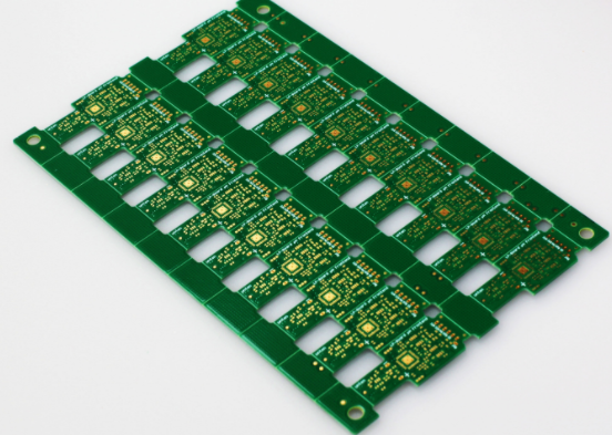
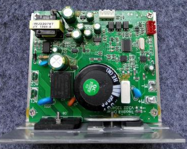
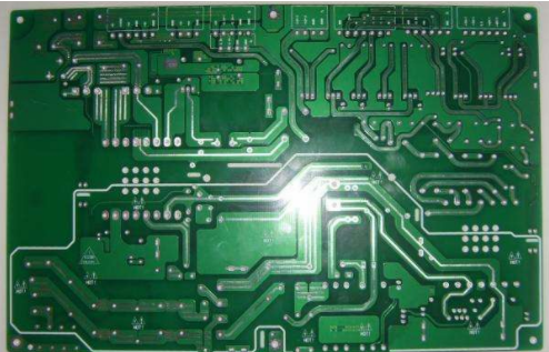
Continue to the back of the board. PCB laminated multi-layer circuit board, the circuit board manufacturer that is strong circuit board processing, processing, soft board processing, Rogers circuit board processing, circuit board rapid proofing, the basis of the entire system design of PCB.
If the laminated design is defective, the EMC performance will be maximized.
1. Each wiring layer must have an adjacent reference layer (power or ground layer);
2. The adjacent main power layer and ground layer should be kept at a minimum distance to provide a larger coupling capacitance;
The following lists the stack from two-layer board to ten-layer board: PCB board and double-sided PCB board stack EMI radiation The main reason for this phenomenon is that not only strong electromagnetic radiation is generated,
And make the circuit sensitive to external interference. From the perspective of electromagnetic compatibility, the key signal mainly refers to the signal that generates strong radiation and the signal that can generate strong radiation is generally a periodic signal, such as a clock or an address.
In the 10KHz low-frequency analog design: the power traces on the same layer are routed radially, and the total length of the lines is minimized;
When the power and ground wires are connected, they should be close to each other; place a ground wire beside the key signal wire. This ground wire forms a smaller loop area and reduces the interference of differential mode radiation to the outside world. After a ground wire,
A loop with the smallest area is formed. If the signal circuit is a double-layer circuit board, it can be on the other side of the circuit board, immediately below the signal line, and as wide as possible along one line.
The loop area formed in this way is equal to the thickness of the circuit board multiplied by
1. SIG-GND(PWR)-PWR (GND)-SIG;
2. GND-SIG(PWR)-SIG(PWR)-GND; 1.6mm (62mil) board thickness. Not only is it not conducive to controlling impedance, interlayer coupling and shielding; especially the power ground layer SI EMI performance is not very good, mainly through the wiring and other details to control.
The main ground layer is placed on the connecting layer of the signal layer with the densest signal, which is good for absorbing and suppressing radiation; increase the 20H rule. Place the required power supply copper layer) occasions. The outer layer of the PCB of this scheme is the ground layer, and the middle two layers are the power supply layer.
The power supply on the signal layer is routed with a wide line, which can make the path impedance of the power supply current low, and EMI control. This is the best 4-layer PCB structure available.
Main attention: The middle two layers of signal and power are mixed with 20H trace impedance. The above solution should be very careful to arrange the traces between the power supply and the ground. In addition, the power supply or the copper on the ground layer should be interconnected as much as possible. To ensure connectivity with low frequencies.
The design of 6-layer board recommends the stacking method:
-GND-SIG-PWR-GND-SIG; This laminated scheme can get better signal integrity, the signal layer and the ground layer are paired with the power layer and the ground layer, and the impedance of each wiring layer can be better controlled,
And both ground layers are capable and can provide better signal layers for each signal layer when the power and ground layers are complete-SIG-GND-PWR-SIG-GND; this solution is only suitable for the case where the device density is not very high This kind of laminated layer has and the ground plane of the top and bottom layers is relatively complete, which can be used as a better one.
It should be noted that the power layer should be close to the layer that is not the main component surface, because the bottom EMI performance is better than the first solution.
, The distance between the power supply layer and the ground layer should be minimized to obtain a good 62mil board thickness. Although the layer spacing is reduced, it is not easy to control the distance between the main power supply and the layer to be small.
Comparing the first scheme with the second scheme, the cost of the second scheme is 20H rule
Rule design
A: This is not a good stacking method due to poor electromagnetic absorption and large power supply impedance.
1.Signal 1 component surface, microstrip wiring layer
2. Signal 2 internal microstrip wiring layer, better wiring layer (X direction)
3.Ground
4. Signal 3 stripline routing layer, better routing layer (Y direction)
5.Signal 4 stripline routing layer
6.Power
7. Signal 5 internal microstrip wiring layer
8. The Signal 6 microstrip trace layer is a variant of the third lamination method. Due to the addition of the reference layer, it has better EMI performance.