PCB board impedance test requirements and technology
The article introduces the reasons and trends of the current demand for impedance testing on PCB boards, and at the same time explains and popularizes its testing technology, which can improve PCB companies understanding of on-board impedance testing technology and development trends, and solve the problems in the production and testing of impedance boards. Do theoretical and technical support for problems.
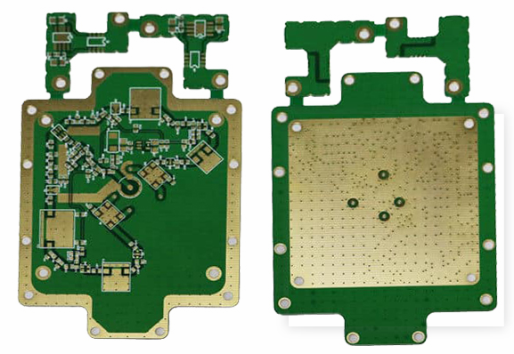
In-board impedance; differential impedance; impedance test 1 Frontier PCB In-board impedance refers to the true impedance of the traces in the finished board, which is not a concept with traditional coupons.
Due to the trace spacing, trace width, trace environment, trace location, and design error between the impedance line in the board and the coupon impedance line, the actual impedance in the board will be different from the coupon impedance.
However, with the current development of circuit boards in the direction of high density, high multi-layers, and small size, customers have increasingly strict requirements for impedance control and higher and higher control accuracy requirements.
This deviation between the on-board impedance and the coupon impedance may be difficult for high-end customers to accept. Therefore, more and more customers require PCB manufacturers to provide real on-board impedance instead of traditional coupons.

On the PCB board, we can see the difference between the impedance line in the Coupon and the real board:
(1) Although the trace spacing and trace width are the same, the spacing of the coupon test points is fixed at 2.54mm (to meet the test probe spacing), and the distance between the end of the real trace (ie gold finger) in the board is variable Yes, with the advent of QFP, PLCC, and BGA packages, the pin pitch of some chips is much smaller than the pitch of 2.54mm (that is, the pitch of the coupon test points).
(2) Coupon routing is an ideal straight line, while the actual routing in the board is often curved and diverse. It is easy for PCB designers and production personnel to idealize the routing of the coupon, but the actual routing on the PCB will cause irregular routing due to various factors.
(3) Coupon and the real wiring in the board have different positions on the entire PCB board. Coupons are located in the middle or edge of the PCB board, and are often removed by the manufacturer when the PCB board leaves the factory. The actual routing positions in the board are diverse, some are near the edge of the board, and some are located in the center of the board.
(4) Vias, pads, shielding layers, etc. are generally distributed around the impedance traces in the board, while the surrounding environment of the Coupon traces is relatively simple. It can be seen that there is a difference between the impedance line in the board and the Coupon trace, and the difference also brings a difference in the impedance test value.
2.2 The influence of impedance test value
(1) Coupon test point spacing The spacing of the coupon traces is different, which will cause impedance discontinuity between the test point and the trace. The distance between the real differential trace ends (ie, the pins of the chip) in the PCB board is often equal to or very close to the trace spacing. This will bring about different impedance test results.
(2) The impedance changes reflected by the curved trace and the ideal trace are inconsistent. The characteristic impedance is often discontinuous where the trace is bent, and the idealized trace of the Coupon cannot reflect the discontinuity of impedance caused by the bending of the trace.
(3) The position of the coupon and the actual trace on the PCB board is different. The current PCB boards are designed with multi-layer wiring, which need to be suppressed during production.
When the PCB board is pressed, the pressure on the different positions of the board cannot be consistent, and the thickness of the dielectric layer at different positions is different. The dielectric constant of the PCB board produced in this way is often different at different positions, and the characteristic impedance is also different. Of course it's different.
(4) The impedance reflected by the internal impedance of the board affected by the surrounding vias, pads, shielding layer, etc. is discontinuous, and the Coupon cannot reflect the true change of impedance due to the single wiring environment. It can be seen that the impedance value reflected by the coupon cannot fully reflect the true characteristic impedance of the real traces in the PCB board.
iPCB is a high-tech manufacturing enterprise focusing on the development and production of high-precision PCBs. iPCB is happy to be your business partner. Our business goal is to become the most professional prototyping PCB manufacturer in the world. Mainly focus on microwave high frequency PCB, high frequency mixed pressure, ultra-high multi-layer IC testing, from 1+ to 6+ HDI, Anylayer HDI, IC Substrate, IC test board, rigid flexible PCB,ordinary multi-layer FR4 PCB, etc. Products are widely used in industry 4.0, communications, industrial control, digital, power, computers, automobiles, medical, aerospace, instrumentation, Internet of Things and other fields.