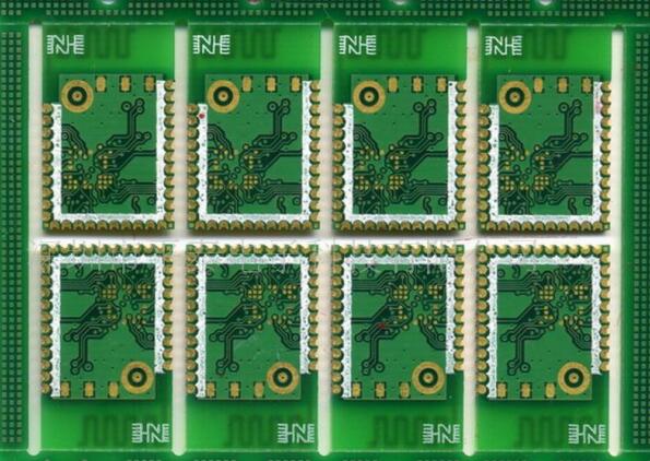
In the circuit board industry, I often hear the term half-hole. Are the holes not all round? Why are there only half-holes? Many friends are not very clear about this. The following editor will talk about it in detail. What is the meaning of a half hole on a circuit board and what issues should be paid attention to when producing a half hole.

Circuit board half hole introduction
Modular PCBs are basically designed with half holes, mainly for easy soldering, small module area, and more functional requirements. The usual half-hole is a hole designed on the most edge of a single PCB, half of the gong is cut in the shape of the gong, leaving only half of the hole on the PCB, commonly known as a half-hole.
Definition of metal half-holes (grooves), once the hole is drilled and then drilled again, the shape process, and finally half of the metalized hole (groove) is retained. Simply put, the metalized hole on the edge of the board is cut in half, and the edge of the board is half-metalized. Hole processing is already a very mature process.
Pay attention to the half-hole technology of circuit board
All metallized half-hole PCB holes must be drilled in the pattern after plating, and before etching, drill one hole at the intersection of both ends of the half hole.
1. The engineering department formulates the MI process according to the half hole process.
2. The metal half-hole is the second-drilled half-hole drilled during the first drilling (or gong), after the image is plated, and before the etching. It must be considered whether the copper will be exposed when the gong groove is shaped, and the drilled half-hole is moved into the unit.
3, right hole (drilled half hole)
A. Finish drilling first, then flip the board (or mirror direction); drill the left hole
B. The purpose is to reduce the pulling of the hole copper in the half hole by the drill, resulting in the lack of hole copper.
4. The size of the drill nozzle for drilling the half hole depends on the spacing of the contour line.
5. Draw solder mask film, use gong space as stop point and open window to increase 4mil treatment.
Based on many years of production experience, it is recommended that the designer make modifications when designing the circuit and change the distance from the edge line to the hole center. The general design is to place the hole center on the edge line and move the control center down. For example, the diameter of the hole is 1.4mm, the distance between the two holes is 2.54mm, the board edge line is 0.33mm from the center of the through hole, and the board thickness is 0.6mm.
The angle between the tangent of the cut point of the wall and the path of the milling cutter was 90 degrees before, but this time it is about 60 degrees. Because the board edge line is at a certain distance from the center of the through hole, the cutting angle of the milling cutter is changed, and the board thickness is extremely small, so the copper in the hole is not easy to be pulled out. The simultaneous improvement of small batch PCB design and production can greatly improve the production yield of PCB half-hole boards.