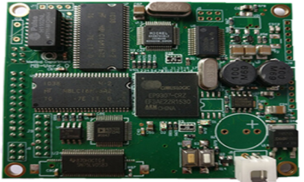
PCB design technology will have an impact on the following three effects:

1. The effect of electrostatic field before electrostatic discharge
2. Charge injection effect caused by discharge
3. Field effect produced by electrostatic discharge current
However, it mainly affects the three effects. The following discussion will give design guidelines for the three mentioned issues.
Generally, the field coupling between receiving circuits can be reduced in one of the following ways:
1. Use a filter at the source to attenuate the signal
2. Use a filter at the receiving end to attenuate the signal
3. Increase the distance to reduce coupling
4. Reduce the antenna effect of the source and/or receiving circuit to reduce coupling
5. Place the receiving antenna and the transmitting antenna vertically to reduce coupling
6. Add shielding between the receiving antenna and the transmitting antenna
7. Reduce the impedance of the transmitting and receiving antennas to reduce electric field coupling
8. Increase the impedance of one of the transmitting or receiving antennas to reduce magnetic field coupling
9. Use a consistent, low-impedance reference plane (as provided by multi-layer PCB design) to couple signals to keep them in common mode
In the specific PCB design, if the electric field or the magnetic field dominate, it can be solved by applying methods 7 and 8. However, electrostatic discharge generally generates an electric field and a magnetic field at the same time, which shows that Method 7 will improve the immunity of the electric field, but at the same time will reduce the immunity of the magnetic field. Method 8 is the opposite of the effect brought by method 7. Therefore, methods 7 and 8 are not perfect solutions. Regardless of whether it is an electric field or a magnetic field, using methods 1 to 6 and 9 will achieve certain results, but the solution of PCB design mainly depends on the combined use of methods 3 to 6 and 9.
The above is the introduction of PCB design technology, Ipcb also provides PCB manufacturers and PCB manufacturing technology.