There are many kinds of PCB production process flow charts. According to the number of layers of the circuit board and the production process of the circuit board, it is divided into: double-sided circuit board process flow, multilayer circuit board process flow, PCB copper electroplating process, CNC numerical control lathe processing process, PCB There are several main production processes for line pattern transfer and shape processing.
The basic manufacturing process of the factory to produce PCB circuit boards
Printed boards can be divided into single-sided, double-sided and multilayer printed boards according to the number of layers of conductor patterns. The basic manufacturing process of a single panel is as follows:
Foil-clad board-->Unloading-->Baking board (to prevent deformation)-->Mould making-->Washing, drying-->Film (or screen printing) ->Exposure and development (or anti-corrosion ink)- ->Etching-->Film removal--->Electrical continuity inspection-->Cleaning treatment-->Screen printing solder mask pattern (printed with green oil)-->Curing-->Screen printing marking symbols-->Curing- ->Drilling-->Shape Processing-->Cleaning and Drying-->Inspection-->Packaging-->Finished Product.
The basic manufacturing process of double-sided panels is as follows:
In recent years, the typical processes for manufacturing double-faced metallized printed boards are the SMOBC method and the pattern plating method. In some specific occasions, the process wire method is also used.

1. Graphic electroplating process
Foil Clad Laminate-->Cutting-->Punching and Drilling Benchmark Holes-->CNC Drilling-->Inspection-->Deburring-->Electroless Plating Thin Copper-->Plating Thin Copper-->Inspecting--> Brushing-->Filming (or screen printing)-->Exposure and developing (or curing)-->Inspection and repairing-->Pattern plating (Cn ten Sn/Pb)-->Removing film-->Etching- ->Inspect and repair the board-->Plug nickel-plated gold- ->Curing-->Shape Processing-->Cleaning and Drying-->Inspection-->Packaging-->Finished Product.
In the process, the two processes of "electroless plating of thin copper --> electroplating of thin copper" can be replaced by a single process of "electroless plating of thick copper", both of which have their own advantages and disadvantages. Pattern electroplating---etching method to make double-faced metallized plates is a typical process in the 1960s and 1970s. In the mid-1980s, the bare copper-clad solder mask process (SMOBC) gradually developed, and has become the mainstream process especially in precision double-sided panel manufacturing.
2. Bare Copper Clad Solder Mask (SMOBC) process
The main advantage of SMOBC board is that it solves the short-circuit phenomenon of solder bridging between thin lines. At the same time, due to the constant ratio of lead to tin, it has better solderability and storage properties than hot melt board.
There are many methods for manufacturing SMOBC boards, including the SMOBC process of standard pattern electroplating subtraction and lead-tin stripping; the subtractive pattern electroplating SMOBC process of using tin plating or immersion tin instead of electroplating of lead-tin; the plugging or masking hole SMOBC process ; Additive method SMOBC technology and so on. The following mainly introduces the SMOBC process and the plugging method SMOBC process flow of the pattern electroplating method and then the lead and tin stripping.
The SMOBC process of pattern electroplating followed by lead and tin stripping is similar to the pattern electroplating process. Changes only after etching.
Double-sided copper clad board-->According to the pattern electroplating process to the etching process-->Pb-Sn-->Inspection-->Cleaning--->Solder mask pattern-->Plug nickel plating and gold plating--> Adhesive tape for plugs-->Hot air leveling-->Cleaning--->Screen printing mark symbols--->Shape processing--->Cleaning and drying--->finished product inspection-->Packaging-->finished product.
PCB process
The film bottom plate is the leading process of printed circuit board production, and the quality of the film bottom plate directly affects the production quality of the printed circuit board. When producing a certain kind of printed circuit board, there must be at least one set of corresponding film masters. Each kind of conductive pattern (signal layer circuit pattern and ground, power layer pattern) and non-conductive pattern (solder mask pattern and character) of the printed board should have at least one film negative. Through the photochemical transfer process, various patterns are transferred to the production board.
The uses of film masters in printed circuit board production are as follows:
The photosensitive mask patterns in pattern transfer include circuit patterns and photoresist patterns.
The production of screen templates in the screen printing process, including solder mask graphics and characters.
Machining (drilling and profile milling) CNC machine tool programming basis and drilling reference.
With the development of the electronics industry, the requirements for printed boards are getting higher and higher. The high-density, fine-wire, and small-aperture designs of printed boards tend to be faster and faster, and the production process of printed boards is becoming more and more perfect. In this case, if there is no high-quality film master, high-quality printed circuit boards can be produced. The production of modern printed boards requires the film master to meet the following conditions:
The dimensional accuracy of the film master must be consistent with the accuracy required by the printed board, and compensation should be made taking into account the deviation caused by the production process.
The graphics of the film base should meet the design requirements, and the graphics symbols should be complete.
The edges of the graphics of the film master are straight and neat, and the edges are not imaginary; the black and white contrast is large, which meets the requirements of the photosensitive process.
The film base material should have good dimensional stability, that is, small dimensional changes due to changes in ambient temperature and humidity.
The film masters of double-sided and multi-layer boards require good overlap of pads and common patterns.
Each layer of the film master should be clearly marked or named.
The film base can transmit the required wavelength of light, and the wavelength range required for general photosensitive is 3000-4000A.
In the past, when making film masters, it was generally necessary to produce a photo master first, and then use photography or pirating to complete the production of the film master. This year, with the rapid development of computer technology, the production process of film masters has also developed greatly. The use of advanced laser light painting technology greatly improves the production speed and the quality of the master, and can produce high-precision, thin-wire patterns that could not be completed in the past, making the CAM technology of printed board production tend to be perfect
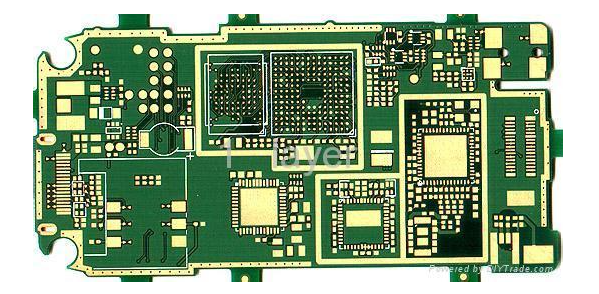
Copper Clad Laminates (Copper Clad Laminates, abbreviated as CCL), referred to as copper clad laminate or copper clad laminate, is the substrate material for manufacturing printed circuit boards (hereinafter referred to as PCB). At present, the most widely used PCB made by etching method is to selectively etch on the copper clad board to obtain the pattern of the required circuit. The copper clad laminate is mainly responsible for the three functions of conduction, insulation and support on the entire printed circuit board. The performance, quality and manufacturing cost of printed boards depend to a large extent on copper clad laminates.
The main process flow of the plugging method is as follows:
Double-sided Foil Clad Laminate-->Drilling-->Chemical Copper Plating-->Plating Copper on the Whole Board-->Blocking Holes-->Screen Printing Imaging (Erect Image)-->Etching-->Removing Screen Printing, Remove plugging material-->Cleaning-->Solder mask pattern-->Plug nickel plating, gold plating-->Plug tape tape-->Hot air leveling-->The following procedures are the same as the above to the finished product.
The process steps of this process are relatively simple, and the key is to plug the holes and clean the ink that plugs the holes.
In the hole plugging process, if the hole plugging ink and screen printing imaging are not used, a special masking dry film is used to cover the hole, and then exposed to make a positive image, this is the masking hole process. Compared with the hole blocking method, it no longer has the problem of cleaning the ink in the hole, but it has higher requirements for masking the dry film.
The basis of the SMOBC process is to first produce a bare copper hole metallized double-sided board, and then apply a hot air leveling process.
PCB engineering production
For the production of PCB printed boards, because many designers do not understand the production process of circuit boards, the circuit diagrams designed by them are only the most basic circuit diagrams and cannot be directly used in production. Therefore, it is necessary to modify and edit the circuit file before actual production. Not only need to make a film chart suitable for the factory's production process, but also need to produce corresponding punching data, mold opening data, and other data useful for production. It is directly related to various future production projects. All of these require engineering and technical personnel to understand the necessary production processes and master related software production, including common circuit design software such as: Protel, Pads2000, Autocad, etc., and also to be familiar with necessary CAM software such as: View2001, CAM350; GCCAM And so on, CAM should include PCB design input, which can edit, correct, repair and imposition circuit graphics, use disk as a medium material, and output automated data for light drawing, drilling, and testing.