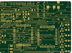
Printed circuit boards, also known as printed circuit boards, are providers of electrical connections for electronic components. Its development has a history of more than 100 years; its design is mainly layout design; the main advantage of using circuit boards is to greatly reduce wiring and assembly errors, and improve the level of automation and production labor rate.
With the continuous progress of PCB technology, the printed circuit board (PCB) industry has been able to develop rapidly, and at the same time, the competition of products has become increasingly fierce, and the PCB industry has entered an era of meager profit. For companies to survive and develop in competition, product manufacturability and cost control are particularly important. However, it has become very difficult for companies to gain competitive advantages from technology and craftsmanship. However, engineering design is the front end of the product manufacturing process. It is very important to fully consider the material cost of the product on the premise of meeting customer requirements during product design. The manufacturing process is difficult, avoiding the extreme capacity of the product, and ensuring the smooth production process of the product. effect. Below we introduce how to reduce the cost in the PCB manufacturing process.

Printed circuit board size optimization Generally speaking, the smaller the printed circuit board size, the lower the cost, but it is not an absolute linear relationship. This has a certain relationship with the cutting process of printed circuit board manufacturing. Therefore, when selecting the estimated printed circuit board size before design, you need to confirm the price of each size with the purchasing department first, and then pre-select the most economical one that meets the needs. size. The best imposition size of the processing board can be determined according to the order category and processing ability, operating skills. Processing imposition is beneficial to improve material utilization, improve efficiency, and save water and electricity consumption. However, imposition size processing will bring about handling, scratching, operation problems, and even a short-term increase in the scrap rate, making quality control more difficult. The engineering review should proceed from the actual situation and determine the best processing board size.
When starting the printed circuit board layout design, in addition to the architectural design based on the functional design requirements, in order to save cost, you need to consider the following aspects: Consider the same circuit diagram design and correspond to multiple similar products. Similar products require different or similar designs due to differences in PCB size, sales area, function, and product grade positioning. If the wiring design of two printed circuit boards is carried out due to a small amount of difference, first, you need to apply for two or more printed circuit board designs, which will incur an additional design cost; secondly, the printed circuit board design After completion, in order to ensure the quality of the product, each printed circuit board needs to be tested for reliability and electrical performance, and additional costs will be incurred for the trial investment in the prototype and the experiment itself.
In addition, the original size of the copper-clad board is too large and inconvenient to process, and sometimes it cannot even be placed in the printed circuit board processing equipment for processing. Therefore, it is necessary to first cut it into several processing-size copper-clad boards. As for the specific size of the processing size, it needs to be determined according to the processing equipment used to make the printed circuit board, the size of each printed circuit board, and some process parameters. In addition to the length and width required for the printed circuit pattern itself, these process parameters also include the width consumed by the screw holes for fixing the printed circuit board on the electronic product frame, the process allowance for shape processing, electroless plating, electroplating and corrosion The remaining amount of clamps when holding, the remaining amount of positioning pins when multi-layer PCB boards, the remaining amount of alignment marks between layers, the remaining amount of logo of the printed circuit board manufacturer, the side width of the printed circuit board, etc., some of them The recommended values of process parameters can be obtained from the copper-clad laminate manufacturer or distributor. When the printed circuit is produced and processed, the above data can be used to determine how many pieces of the processing size of the copper-clad laminate are to be cut from a large original size copper-clad laminate, whether it is vertical or horizontal, whether it can be cut, and so on.